
Tantalum compound, method for producing same, tantalum-containing thin film and method for forming same

a technology of tantalum compound and thin film, applied in the field of tantalum compound and a method for producing the same, can solve the problems of degradation of the performance of the insulating film, delay of signal transmission, and generation of defects

Active Publication Date: 2009-09-22
SAGAMI CHEM RES CENT +1
View PDF7 Cites 3 Cited by
  • Summary
  • Abstract
  • Description
  • Claims
  • Application Information

AI Technical Summary

Benefits of technology

The present invention relates to a new tantalum compound and a method for producing it. This compound can be used to form thin films by chemical vapor deposition or atomic layer deposition methods, which are useful for the production of semiconductor devices. The new compound does not contain halogens or nitrogen, which makes it easier to vaporize and use in chemical vapor deposition methods. The invention also provides a method for using an organometallic compound as a raw material for the formation of tantalum films, which is more stable and easier to vaporize than other tantalum compounds. The new compound can be used to prevent the diffusion of copper in insulating films, which is important for the performance of semiconductor devices.

Problems solved by technology

Width of wiring in a device becomes fine, and aluminum conventionally used as a wiring material gives rise a problem in delay of signal transmission.
Copper has the characteristic that resistance is low, but has the disadvantage that it is liable to be diffused in a silicon oxide used in an insulating film between wirings, resulting in degradation of performance of the insulating film.
However, the tantalum nitride film has poor adhesion to a copper seed film for forming a copper wiring by plating, and film peeling occurs between the tantalum nitride film and the copper seed film when forming a wiring or planarizing after wiring formation, resulting in generation of defect.
In the PVD method, it is difficult to form a uniform film on a concave-convex surface, and from now, where miniaturization of a semiconductor device is advanced, it will be required to form a uniform and thin film on a surface of a complicated three dimensional structure.
However, the halide has high melting point and is required to vaporize by sublimation.
Thus, it is difficult to use the halide as a raw material in CVD method or ALD method.
Additionally, there are the problems on corrosion of a film due to a residual halogen in a film, deterioration of adhesion and the like.
On the other hand, in the amide compound, because nitrogen remains in a film, it is possible to form a tantalum nitride film, but it is difficult to form a metallic tantalum film.
However, there are the problems that those tantalum compounds have low heat stability, and are difficult to vaporize stably.

Method used


Image

  • Tantalum compound, method for producing same, tantalum-containing thin film and method for forming same
  • Tantalum compound, method for producing same, tantalum-containing thin film and method for forming same
  • Tantalum compound, method for producing same, tantalum-containing thin film and method for forming same

Examples


example 1

Synthesis of trihydridobis(propylcyclopentadienyl)tantalum (Ta(PrCp)2H3)

[0052]80.0 g (223 mmol) of tantalum pentachloride was suspended in 1,340 ml of ether, and 324 ml (220 mmol) of isopropyl magnesium bromide (0.68M THF solution) was added thereto. A solution of 50.2 g (440 mmol) of propylcyclopentadienyl lithium prepared from propylcylopentadiene and butyl lithium in THF (380 ml) was added, followed by refluxing for 1 hour. The solvent was distilled away, and the residue was dried at 80° C. in vacuo for 8 hours to obtain a brownish-red solid containing dichlorobis(propylcyclopentadienyl)tantalum (Ta (PrCp)2Cl2). 2,100 ml of toluene was added to this brownish-red solid, and the resulting mixture was ice-cooled. 198 ml (660 mmol) of a toluene solution (65 wt %) of sodium bis(2-methoxyethoxy)aluminum hydride was added dropwise to the mixture, and temperature was returned to room temperature, followed by stirring for 19.5 hours. 106 ml of water was added to the mixture, followed by s...

example 2

Synthesis of hydridobis(propylcyclopentadienyl)carbonyl-tantalum (Ta(PrCp)2(CO)H)

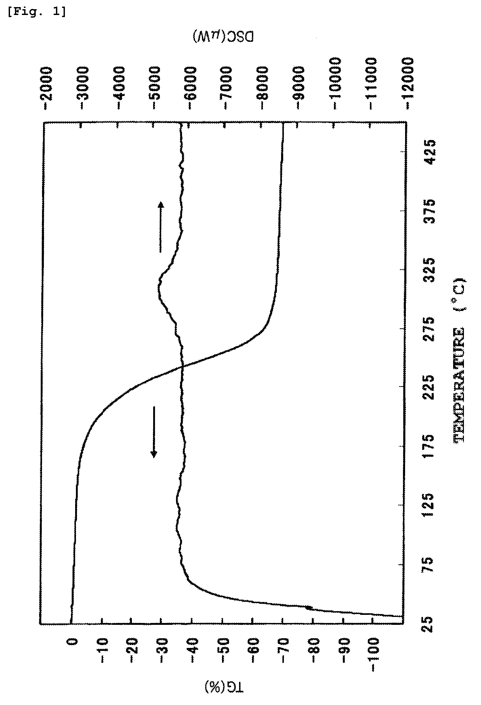
[0054]11.2 g (28.1 mmol) of trihydridobis(propyl-cyclopentadienyl)tantalum was heated to 135° C. in nonane (200 ml) under a carbon monoxide atmosphere, and stirred for 4 hours. The solvent was distilled away from the reaction mixture, and a solution hexane-extracted from the residue was concentrated to about 200 ml, and then cooled to −70° C. The supernatant was removed, and the solid was washed with 20 ml of hexane two times, and dried in vacuo to obtain 7.45 g (yield: 62.4%) of a purple solid. Thermal analysis result of the tantalum compound obtained is shown in FIG. 1. It is seen from this Figure that the tantalum compound obtained has a wide temperature range at which the compound can vaporize stably without decomposition, and thermally decomposes in the vicinity of 260° C., and the compound is therefore suitable as a raw material of a tantalum-containing thin film by CVD method or ALD method.

[0055]...

example 3

Synthesis (1) of bis(ethylcyclopentadienyl)trihydrido-tantalum (Ta(EtCp)2H3)

[0063]75.0 g (209 mmol) of tantalum pentachloride was suspended in 1,200 ml of ether, and 335 ml (228 mmol) of isopropyl magnesium bromide (0.68M THF solution) was added thereto. A solution of 41.9 g (419 mmol) of ethylcylopentadienyl lithium prepared from ethylcylopentadiene and butyl lithium in THF (240 ml) was added, followed by refluxing for 1 hour. The solvent was distilled away, and the residue was dried at 80° C. in vacuo for 8 hours to obtain a dark brown solid containing bis(ethylcyclopentadienyl)dichlorotantalum (Ta(EtCp)2Cl2). 1,060 ml of toluene was added to this dark brown solid, and the resulting mixture was ice-cooled. 187 ml (623 mmol) of a toluene solution (65 wt %) of sodium bis(2-methoxyethoxy)aluminum hydride was added dropwise to the mixture, and temperature was returned to room temperature, followed by stirring for 17 hours. 107 ml of water was added to the mixture, followed by stirring...


PUM

PropertyMeasurementUnit
melting pointaaaaaaaaaa
temperatureaaaaaaaaaa
boiling pointaaaaaaaaaa

Abstract

A novel tantalum compound, a method for producing the novel tantalum compound, and a method for stably forming a tantalum-containing thin film which contains the desired element. The tantalum compound enables one to selectively form a tantalum-containing thin film free of halogen and the like, and various tantalum-containing thin films which contain the desired element.

Description

TECHNICAL FIELD[0001]The present invention relates to a novel tantalum compound and a method for producing the same. The tantalum compound of the present invention is useful for the formation of a tantalum-containing thin film by a chemical vapor deposition method (CVD method) or an atomic layer deposition method (ALD method). Further, it relates to a method for forming a tantalum-containing thin film which is useful for the production of semiconductor devices, and a tantalum-containing thin film.BACKGROUND ART[0002]Miniaturization of device structure is advanced with enhanced performance of semiconductor devices. Width of wiring in a device becomes fine, and aluminum conventionally used as a wiring material gives rise a problem in delay of signal transmission. As a result, copper has been used. Copper has the characteristic that resistance is low, but has the disadvantage that it is liable to be diffused in a silicon oxide used in an insulating film between wirings, resulting in de...

Claims


Application Information

Patent Timeline
Patent Type & Authority Patents(United States)
IPC IPC(8): C07F17/00C23C16/00H01L21/4763
CPCC23C16/18C07F17/00C07F9/00C07F19/00C23C16/00H01L21/44
Inventor SEKIMOTO, KENICHITADA, KEN-ICHITAKAMORI, MAYUMIYAMAKAWA, TETSUFURUKAWA, TAISHIOSHIMA, NORIAKI
Owner SAGAMI CHEM RES CENT
Learn More