


Quick Research
Generate reliable direction feasibility study reports for your R&D in just a few steps.

Technical Q&A
Discover and master advanced knowledge NOW. Basics, ideas, possibilities, all at once.

Find Solutions
As an expert in R&D theories, this can generate solutions to your technical problems instantly.

Evaluate Feasibility
Analyze your overall solution with one click, know your potential R&D risks in advance.

Monitor Landscape
Get weekly tech updates, stay abreast of the latest tech innovations and key insights.
Method of manufacturing ferroelectric semiconductor device
a technology of ferroelectric semiconductors and manufacturing methods, applied in the direction of capacitors, digital storage, instruments, etc., can solve the problems of ferroelectric film, no heat treatment, no heat treatment, etc., and achieve the effect of suppressing removal and mutual diffusion of constituent elements
- Summary
- Abstract
- Description
- Claims
- Application Information
AI Technical Summary
Benefits of technology
Problems solved by technology
Method used
Image

Examples
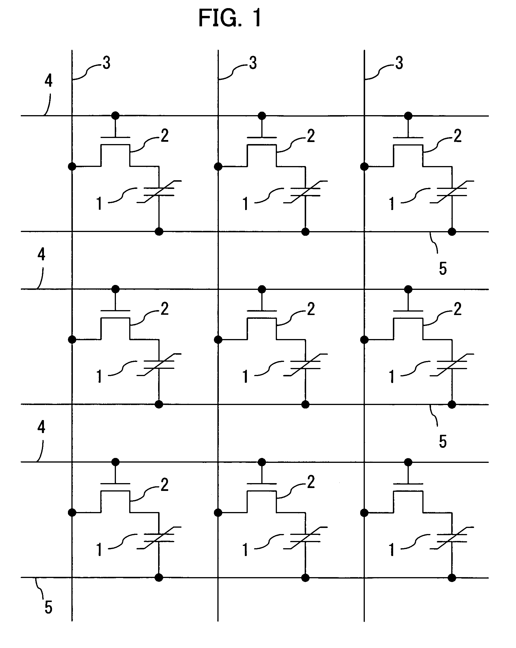
first embodiment
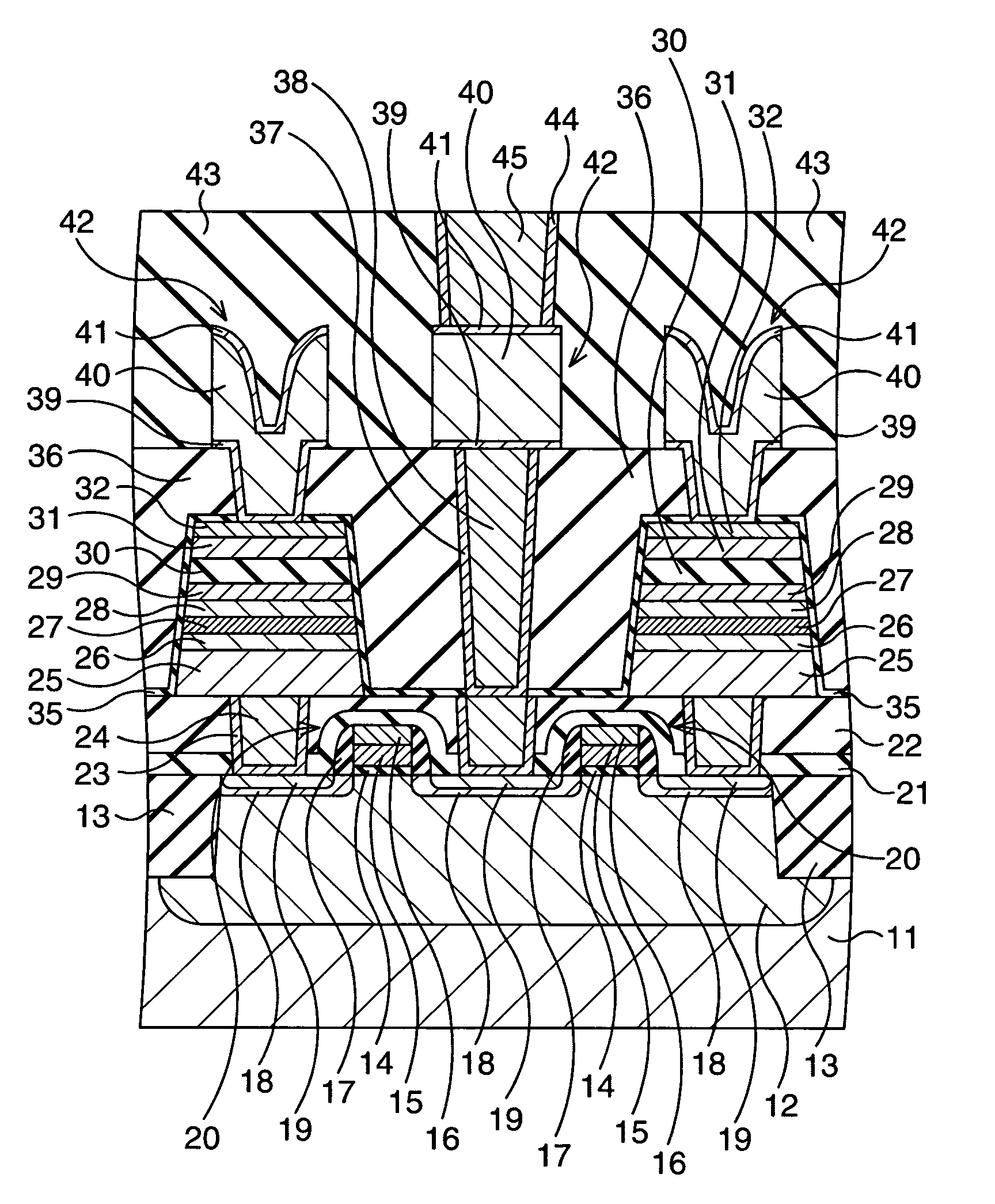
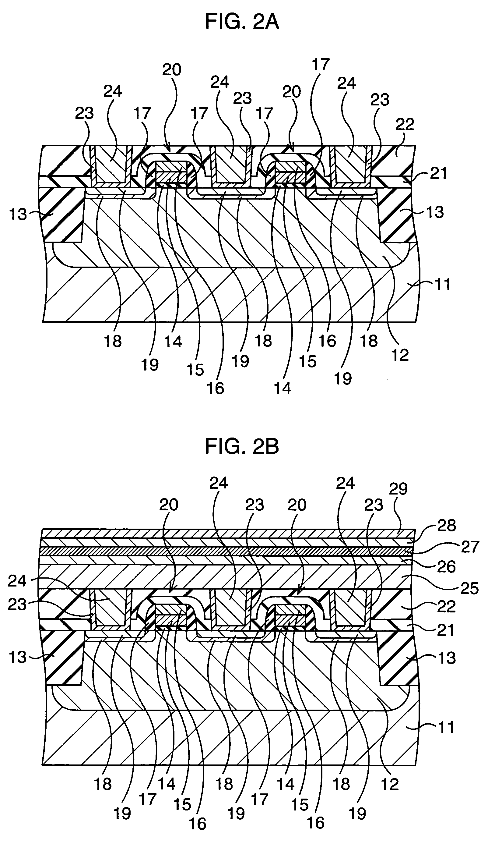
[0038]Next, a first embodiment of the present invention will be described. FIG. 2A to FIG. 2D are cross-sectional views showing, in the order of steps, a method of manufacturing a ferroelectric memory (semiconductor device) according to the first embodiment of the present invention. However, FIG. 2A to FIG. 2D show the cross section perpendicular to the direction in which the bit line 3 extends. Further, FIG. 2A to FIG. 2D show a portion corresponding to two MOS transistors sharing one bit line (corresponding to the bit line 3 in FIG. 1).
[0039]In the first embodiment, as shown in FIG. 2A, a well 12 is first formed in the surface of a semiconductor substrate 11 such as a silicon substrate. Then, in the surface of the semiconductor substrate 11, element isolation regions 13 are formed, for example, by an STI (shallow trench isolation) Subsequently, gate insulation films 14, gate electrodes 15, cap films 16, side walls 17, source / drain diffusion layers 18, and silicide layers 19 are fo...
second embodiment
[0054]Next, a second embodiment of the present invention will be described. The first embodiment is made by applying the present invention to the stack-structure ferroelectric capacitor, while the second embodiment is made by applying the present invention to a planar-structure ferroelectric capacitor. FIG. 3A and FIG. 3B are cross-sectional views showing, in the order of steps, a method of manufacturing a ferroelectric memory (semiconductor device) according to the second embodiment of the present invention.
[0055]In the second embodiment, as shown in FIG. 3A, processing from the formation of the well 12 to the formation of the W-plugs 24 is performed first as in the first embodiment.
[0056]Then, a lower electrode adhesion film 64 and a Pt film 61 are formed in sequence on the entire surface. The lower electrode adhesion film 64 and Pt film 61 (lower electrode film) are formed, for example, by the sputtering method. The thickness of the lower electrode adhesion film 64 is, for exampl...
PUM
| Property | Measurement | Unit |
|---|---|---|
| thickness | aaaaa | aaaaa |
| thickness | aaaaa | aaaaa |
| temperature | aaaaa | aaaaa |
Abstract
Description
Claims
Application Information
 - R&D Engineer
- R&D Manager
- IP Professional
- Industry Leading Data Capabilities
- Powerful AI technology
- Patent DNA Extraction
Browse by: Latest US Patents, China's latest patents, Technical Efficacy Thesaurus, Application Domain, Technology Topic, Popular Technical Reports.
© 2024 PatSnap. All rights reserved.Legal|Privacy policy|Modern Slavery Act Transparency Statement|Sitemap|About US| Contact US: help@patsnap.com