Metal interconnect structure and method

a technology of metal interconnects and metal plates, applied in the direction of semiconductor devices, semiconductor/solid-state device details, electrical apparatus, etc., can solve the problems of reducing yields, achieve greater mechanical stability, improve the capacitive delay of chip level interconnects, and weaken the mechanical stability of stacks

Active Publication Date: 2008-02-19
INFINEON TECH AG
View PDF28 Cites 26 Cited by
  • Summary
  • Abstract
  • Description
  • Claims
  • Application Information

AI Technical Summary

Benefits of technology

[0020]Embodiments of the invention are useful since they are especially tailored for use with low-k dielectrics. Low k dielectrics can be used to improve the capacitive delay in the chip level interconnect. Use of aspects of the present invention can provide greater mechanical stability when using low-k materials, since these materials my have free volume (e.g., voids or pores) that lead to weaker mechanical stability of the stack.
[0021]In another aspect, the present invention provides improved electrical conductivity between levels of metal since the higher resistance liner can be removed or reduced.

Problems solved by technology

When a device comprises multiple metallization and dielectric layers, the solvent-removing heating step for the low-dielectric constant material layers must be repeated numerous times (e.g., each layer must be cured), which can be problematic, especially for the lower layers of the device.
The mismatch of thermal expansion coefficients of metal leads and low-k dielectric layers causes thermo-mechanical stress, leading to increased resistances, delaminations, electrical intermittencies and opens, resulting in reduced yields.

Method used


Image

  • Metal interconnect structure and method
  • Metal interconnect structure and method
  • Metal interconnect structure and method

Examples


Embodiment Construction

[0029]The making and using of the presently preferred embodiments are discussed in detail below. It should be appreciated, however, that the present invention provides many applicable inventive concepts that can be embodied in a wide variety of specific contexts. The specific embodiments discussed are merely illustrative of specific ways to make and use the invention, and do not limit the scope of the invention.

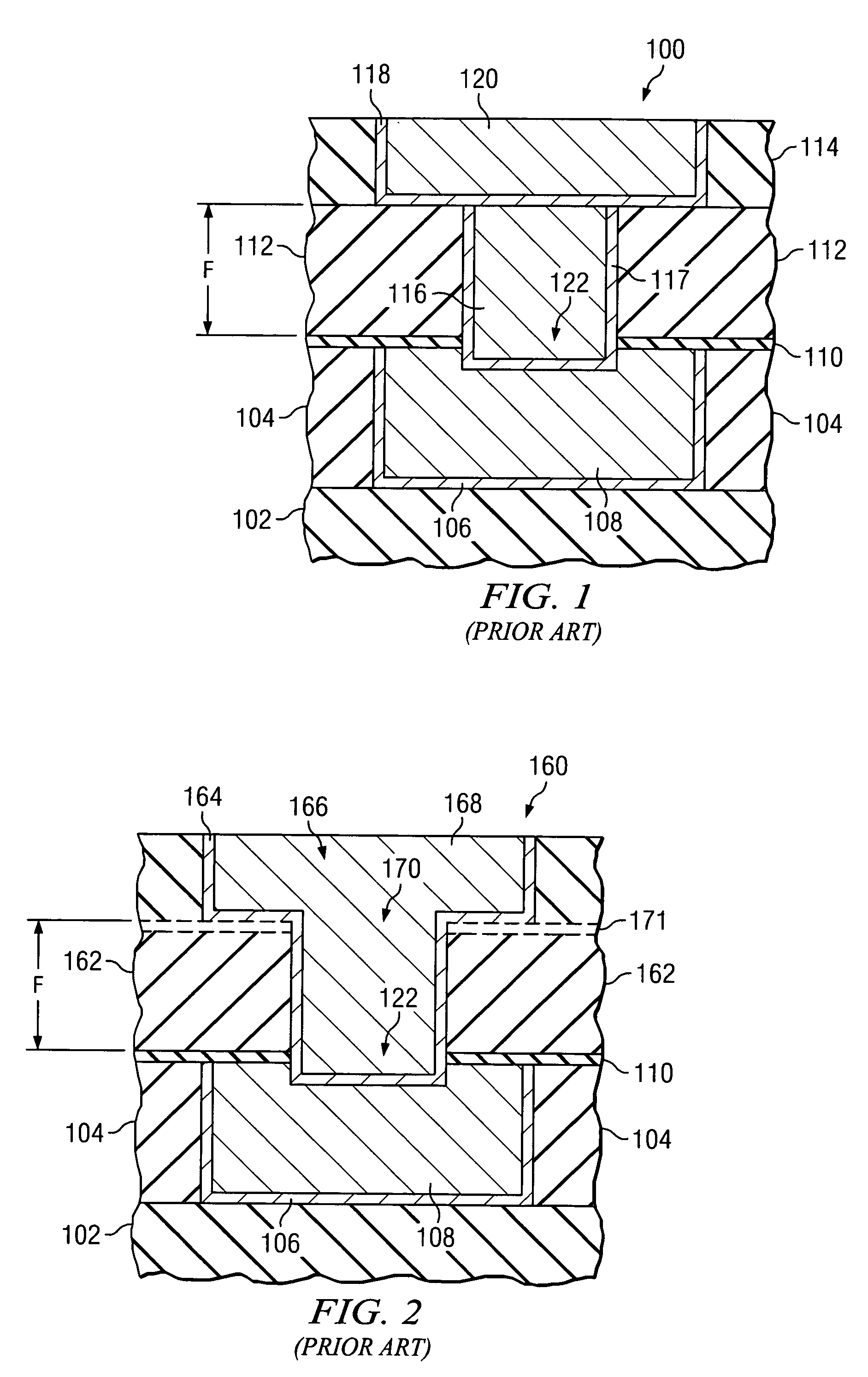
[0030]The present invention will be described with respect to preferred embodiments in a specific context, namely a dual damascene metallization scheme. The invention may also be applied, however, to other interconnect structures.

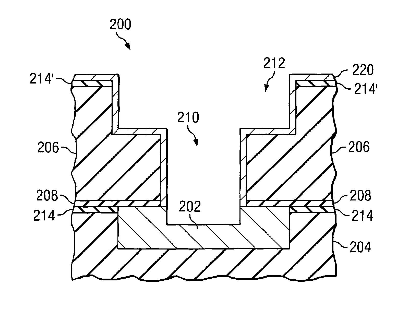
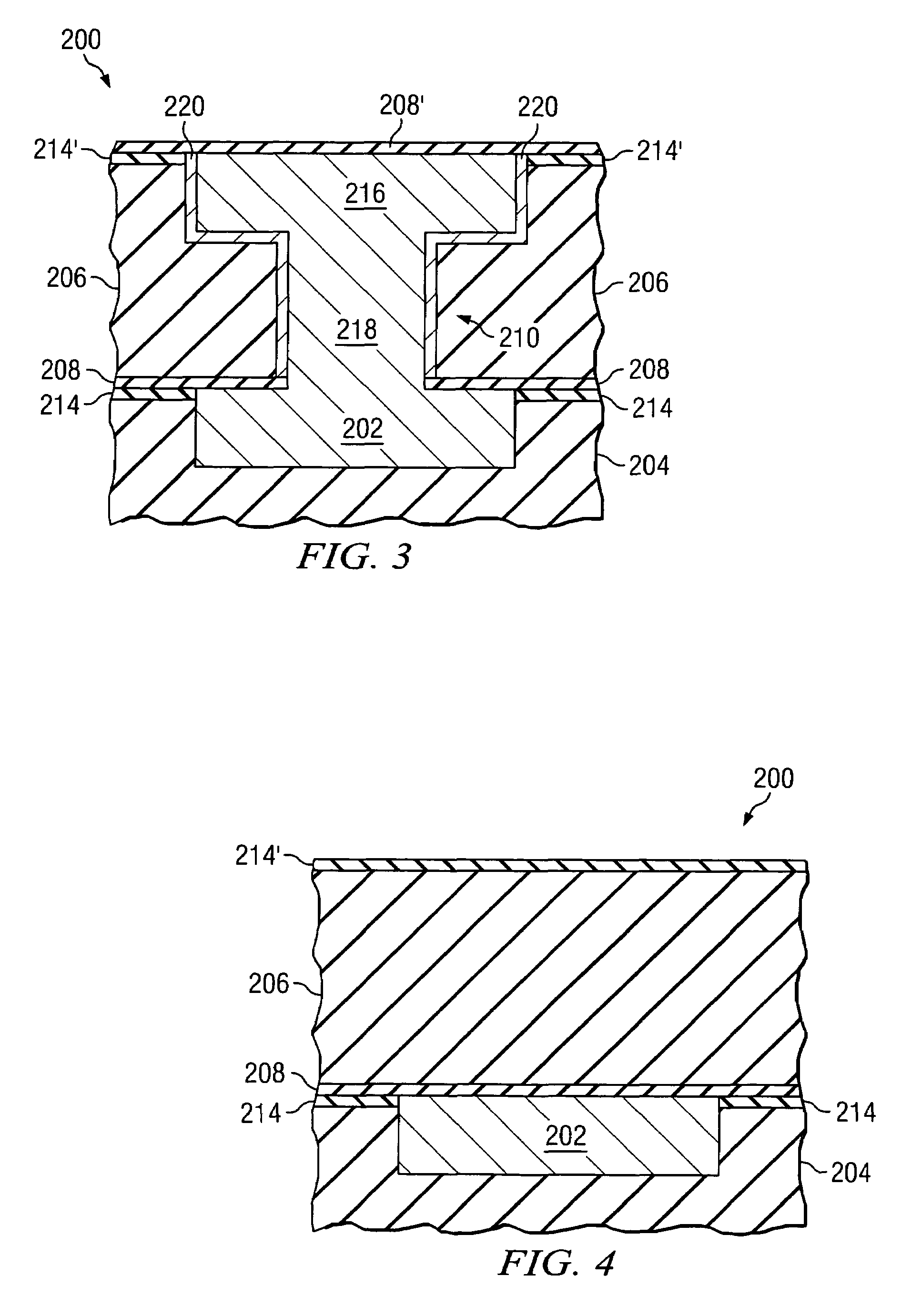
[0031]A preferred embodiment interconnect structure is illustrated in FIG. 3. One embodiment for fabricating this structure is illustrated in FIGS. 4-9. As will be explained below, and as would be understood by one of ordinary skill in the art, various modifications of the specific structure and process are possible.

[0032]Referring first to FIG. 3, a...


PUM


Abstract

In a method of fabricating a semiconductor device, a dielectric layer is formed over a conductive region. A dual damascene structure including a trench and a via is formed within the dielectric layer. A liner is formed over the dual damascene structure. The liner is selectively removed from above the upper surface of the conductive region to expose the upper surface of the conductive region. After the selectively removing process, at least a portion of the liner remains over the lower surface of the trench and the sidewalls of the trench and the via hole. A wet etch can then be performed to etch a recess in the conductive region. A conductive material is then formed within the damascene structure. This conductive material physically contacts the conductive region and is separated from the dielectric layer by the remaining portion of the liner.

Description

TECHNICAL FIELD[0001]The present invention relates generally to semiconductor devices and methods, and more particularly to a metal interconnect structure and method.BACKGROUND[0002]Semiconductors are widely used for integrated circuits for electronic applications, including radios, televisions and personal computing devices, as examples. Such integrated circuits typically use multiple transistors fabricated in single crystal silicon. It is common for there to be millions of semiconductor devices on a single semiconductor product. Many integrated circuits now include multiple levels of metallization for interconnections.[0003]The semiconductor industry continuously strives to decrease the size of the semiconductor devices located on integrated circuits. Miniaturization is generally needed to accommodate the increasing density of circuits necessary for today's semiconductor products. In the past, the material typically used to isolate conductive leads from each other has been silicon...

Claims


Application Information

Patent Timeline
Patent Type & Authority Patents(United States)
IPC IPC(8): H01L23/48
CPCH01L21/76805H01L21/76838H01L21/76843H01L21/76844H01L21/76873H01L23/5226H01L23/53238H01L23/53295H01L2924/0002H01L2924/00
Inventor BECK, MICHAEL
Owner INFINEON TECH AG
Why Eureka
Try Eureka