Magnetic sensing element including magnetic layer composed of Heusler alloy disposed on underlayer having {111}-oriented fcc structure
a magnetic layer and sensing element technology, applied in the field can solve the problems of considerable limitations in the design of magnetic sensing elements reduce spin-independent scattering of conduction electrons, and increase the change ratio of magnetoresistance
- Summary
- Abstract
- Description
- Claims
- Application Information
AI Technical Summary
Benefits of technology
Problems solved by technology
Method used
Image


Examples
first embodiment
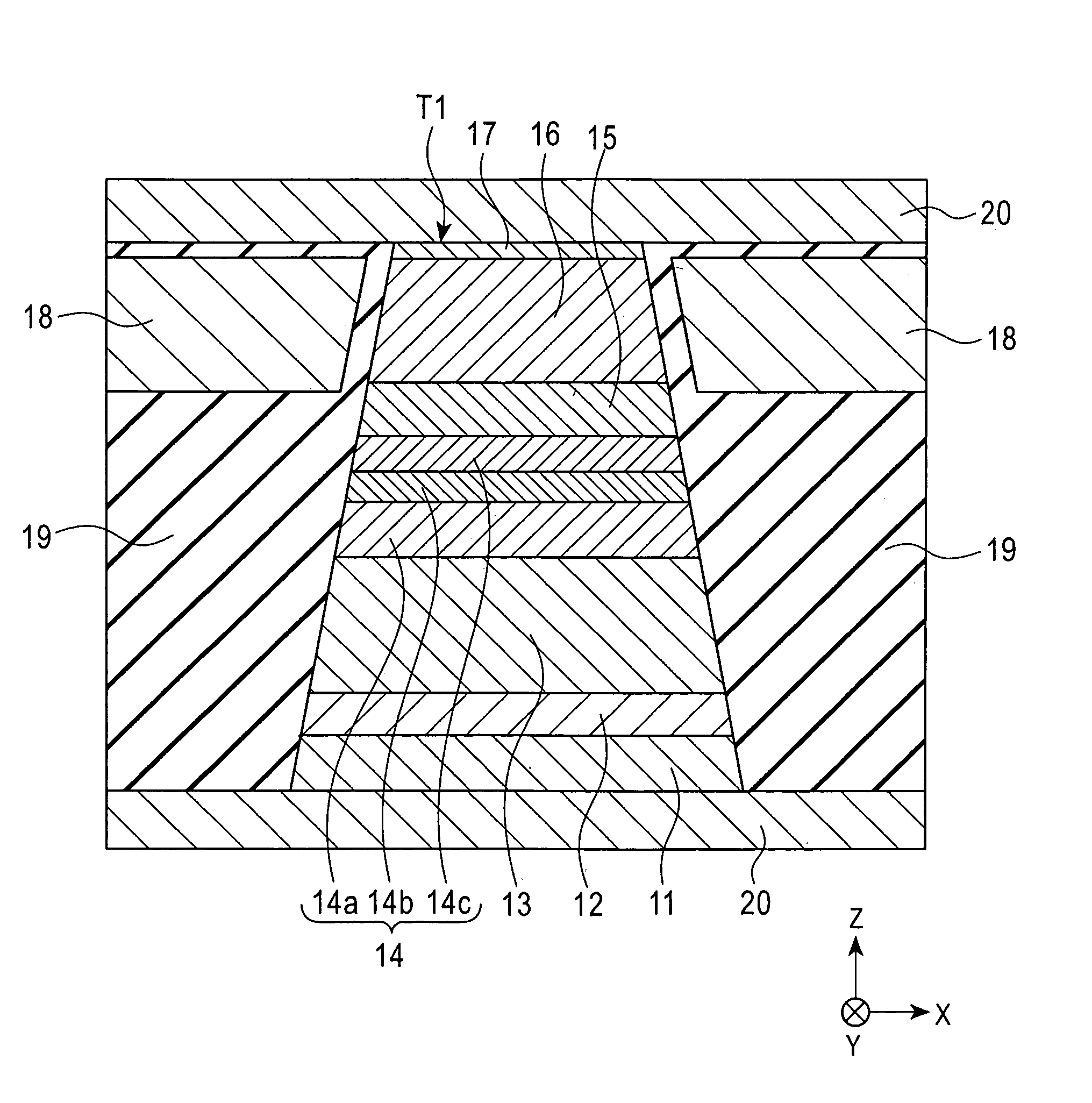
[0053]FIG. 1 is a cross-sectional view of an overall structure of a magnetic sensing element (single spin-valve magnetoresistive element) according to a first embodiment of the present invention, viewed from a surface facing a recording medium. FIG. 1 shows only the central portion of the sensing element expanding in the X direction.
[0054]For example, this single spin-valve magnetoresistive element is mounted at the trailing edge of a floating slider installed in a hard disk device to detect magnetic fields recorded on a hard disk. A magnetic recording medium such as a hard disk moves in the Z direction, and the leakage magnetic field from the magnetic recording medium is in the Y direction.
[0055]Referring to FIG. 1, a base layer 11 is deposited at the bottom. The base layer 11 is composed of a nonmagnetic material, for example, at least one element selected from Ta, Hf, Nb, Zr, Ti, Mo, and W. A multilayer film T1 is deposited on the base layer 11. The multilayer film T1 includes a ...
second embodiment
[0100]FIG. 2 is a partial cross-sectional view showing a structure of a dual spin-valve magnetic sensing element according to a second embodiment of the present invention.
[0101]Referring to FIG. 2, from the bottom, a base layer 11, a seed layer 12, an antiferromagnetic layer 13, a pinned magnetic layer 31, a nonmagnetic layer 15, and a free magnetic layer 16, which is a Heusler alloy layer, are sequentially deposited. Furthermore, on the free magnetic layer 16, another nonmagnetic layer 15, a pinned magnetic layer 32, another antiferromagnetic layer 13, and a protective layer 17 are sequentially deposited to form a multilayer film T2.
[0102]Hard bias layers 18 are disposed at each end of the free magnetic layer 16. The hard bias layers 18 are insulated by an insulating layer 19 composed of, for example, alumina.
[0103]Electrode layers 20 are disposed on and under the multilayer film T2. The magnetic sensing element of the present embodiment is a CPP-GMR magnetic sensing element in whi...
third embodiment
[0131]FIG. 3 is a partial cross-sectional view showing a structure of a top spin-valve magnetic sensing element according to a third embodiment of the present invention.
[0132]Referring to FIG. 3, from the bottom, a base layer 11, a seed layer 12, a free magnetic layer 41, a nonmagnetic layer 15, a pinned magnetic layer 32, an antiferromagnetic layer13, and a protective layer 17 are sequentially deposited to form a multilayer film T3.
[0133]Hard bias layers 18 are disposed at each end of the free magnetic layer 41. The hard bias layers 18 are insulated by an insulating layer 19 composed of, for example, alumina.
[0134]Electrode layers 20 are disposed on and under the multilayer film T3. The magnetic sensing element of the present embodiment is a CPP-GMR magnetic sensing element in which a sense current flows in the direction perpendicular to the surface of each layer of the multilayer film T3.
[0135]In FIG. 3, layers having the same reference numeral as in FIG. 1 or FIG. 2 are composed ...
PUM
| Property | Measurement | Unit |
|---|---|---|
| Grain size | aaaaa | aaaaa |
| Thickness | aaaaa | aaaaa |
| Antiferromagnetism | aaaaa | aaaaa |
Abstract
Description
Claims
Application Information
 - R&D
- Intellectual Property
- Life Sciences
- Materials
- Tech Scout
- Unparalleled Data Quality
- Higher Quality Content
- 60% Fewer Hallucinations
Browse by: Latest US Patents, China's latest patents, Technical Efficacy Thesaurus, Application Domain, Technology Topic, Popular Technical Reports.
© 2025 PatSnap. All rights reserved.Legal|Privacy policy|Modern Slavery Act Transparency Statement|Sitemap|About US| Contact US: help@patsnap.com