
Anisotropic conductive connector device and production method therefor and circuit device inspection device

a technology of anisotropic conductive connectors and production methods, which is applied in the direction of coupling device connections, instruments, connection contact material materials, etc., can solve the problems of reducing the conductivity of unable to inspect the succeeding circuit device, and generating permanent compressive deformation over the conducting path forming portion, etc., to achieve stably maintain excellent electrical connection state, and be manufactured efficiently and inexpensively.

Active Publication Date: 2007-12-18
ISC CO LTD
View PDF16 Cites 17 Cited by
  • Summary
  • Abstract
  • Description
  • Claims
  • Application Information

AI Technical Summary

Benefits of technology

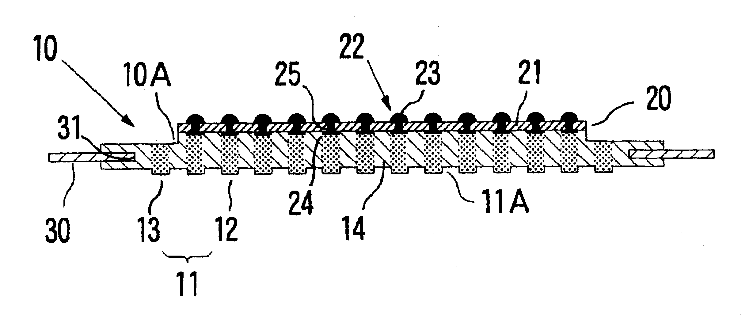
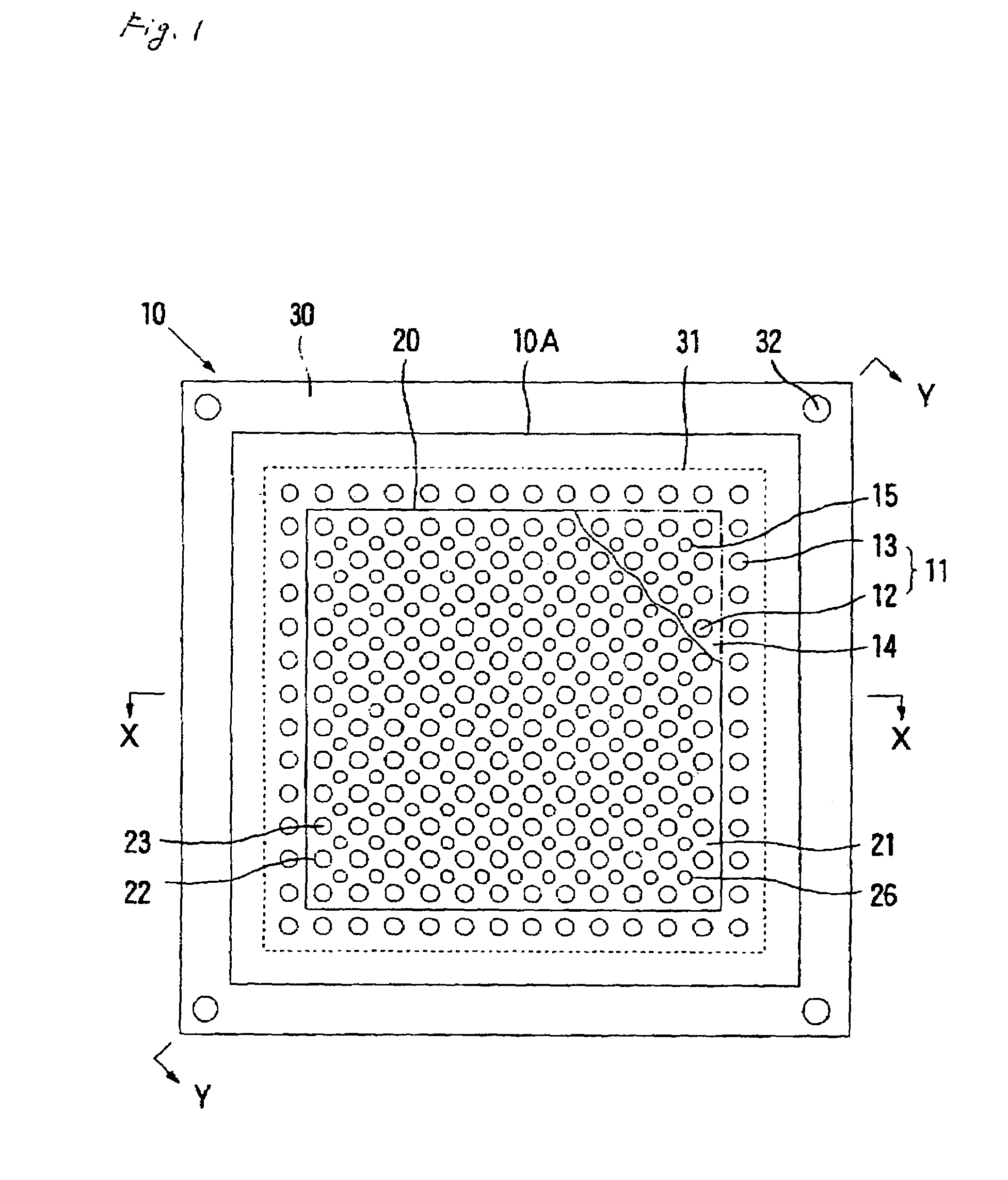
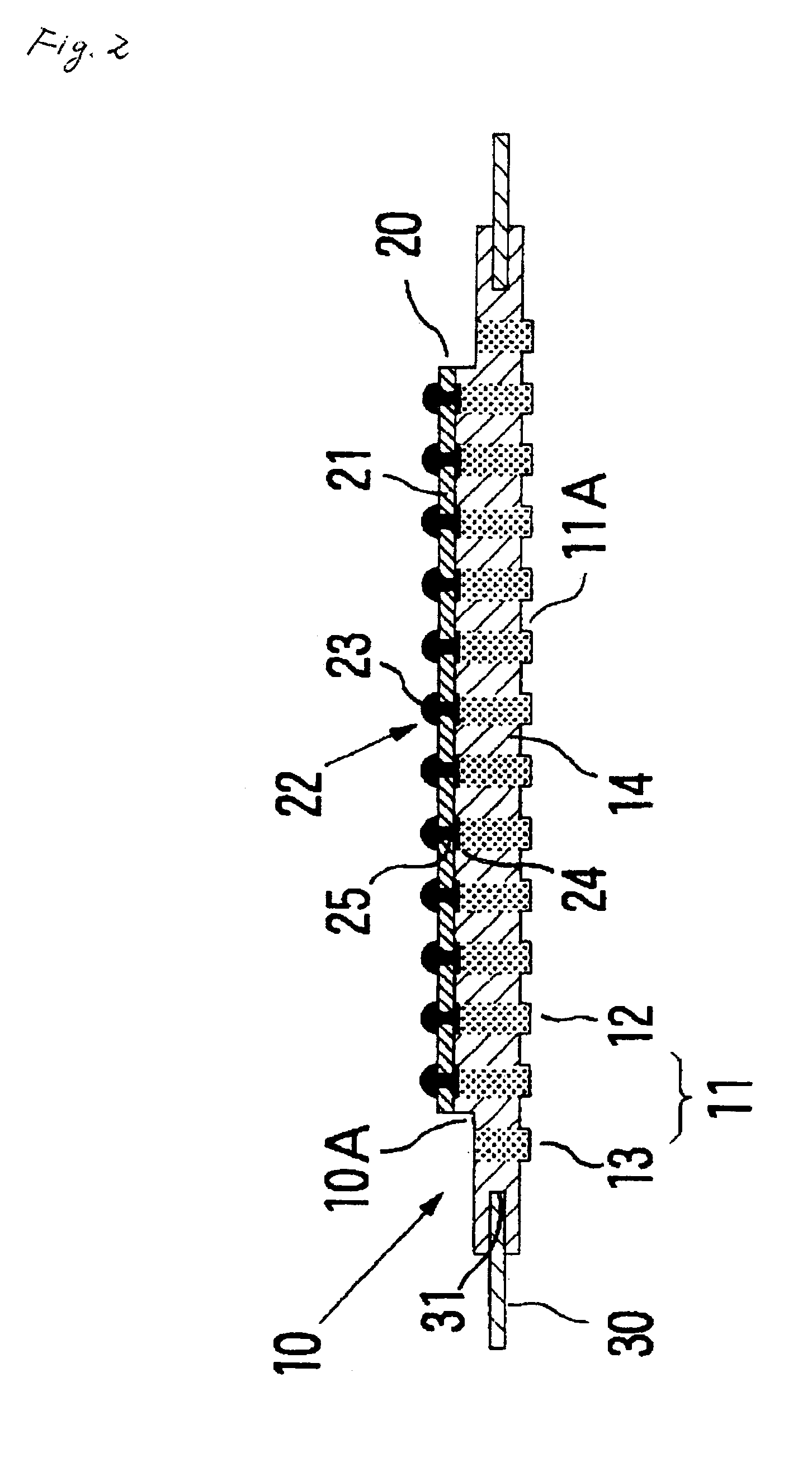
[0135]According to the anisotropic conductive connector device in accordance with the present invention, the sheet-like connector is provided integrally on the anisotropic conductive film or is integrated therewith. Therefore, a work for aligning the sheet-like connector is not required, and even if the pitch of the electrodes to be the connecting object is small, an excellent electrical connection state can be obtained.
[0136]In addition, also in the case of repetitive use for a long period of time or the case of use in a high temperature environment, a positional shift between the conducting path forming portion and the electrode structure is not generated. Accordingly, it is possible to stably maintain the excellent electrical connection state.
[0137]Moreover, according to the anisotropic conductive connector device in accordance with the present invention, the sheet-like connector is obtained by an insulating sheet formed by the mesh, the nonwoven fabric or the porous sheet on which a void communicating with both sides of the insulating sheet is provided. Therefore, a work for forming a through hole is not required in the manufacture of the sheet-like connector. Consequently, the sheet-like connector can be manufactured efficiently and inexpensively. Thus, the anisotropic conductive connector device can also be manufactured efficiently and inexpensively.
[0138]Furthermore, according to the anisotropic conductive connector device in accordance with the present invention, the sheet-like connector is obtained by the insulating sheet formed by the mesh, the nonwoven fabric or the porous sheet. Therefore, When the sheet-like connector is to be integrated with the anisotropic conductive film of the anisotropic conductive connector, the sheet-like connector is disposed on the molding material layer in the metal mold to carry out the curing treatment over the molding material layer. Consequently, an elastically polymeric substance constituting the molding material layer is cured in a permeation state into the mesh or the nonwoven fabric. Thus, it is possible to integrate the sheet-like connector with the anisotropic conductive connector reliably and firmly.
[0139]In the anisotropic conductive connector device in which the sheet-like connector is integrated, thus, also in the case of repetitive use for a long period of time or the case of use in a high temperature environment, a positional shift between the conducting path forming portion and the electrode structure is not generated. Accordingly, it is possible to stably maintain an excellent electrical connection state.
[0140]Furthermore, according to the method of manufacturing an anisotropic conductive connector device in accordance with the present invention, the sheet-like connector is disposed on the molding material layer for obtaining the anisotropic conductive film and the molding material layer is subjected to a curing treatment in this state. Therefore, it is possible to advantageously and reliably manufacture the anisotropic conductive connector device in which the sheet-like connector is provided integrally on the anisotropic conductive film.

Problems solved by technology

However, for example, in an electrical inspection for a circuit device having a protruded electrode formed of a soldering alloy, in the case in which an anisotropic conductive sheet according to the conventional art is to be used as a connector, there is the following problem.
For this reason, there is a problem in that it is hard to inspect succeeding circuit devices.
As a result, there is a problem in that the conductivity of the conducting path forming portion is reduced.
Moreover, for example, in the electrical inspection for a circuit device having a pad electrode formed of aluminum, in the case in which the anisotropic conductive sheet according to the conventional art is used as a connector, there is the following problem.
By repetitively using such an anisotropic conductive sheet, however, a permanent compressive deformation is generated over the conducting path forming portion.
Therefore, the electric resistance value of the conducting path forming portion in the anisotropic conductive sheet is increased or the stable electrical connection of the conducting path forming portion for the pad electrode is not achieved.
Consequently, there is a problem in that it is hard to inspect succeeding circuit devices.
However, in such means, when the pitches of the electrode structure of the sheet-like connector and the conducting path forming portion of the anisotropic conductive sheet are reduced, it is harder to reliably align both of them.
As a result, there is a problem in that an excellent electrical connection state cannot be maintained stably.
For this reason, in the case in which the inspection is carried out repetitively, peeling is easily caused on an interface between the sheet-like connector and the anisotropic conductive sheet and there is caused a conducting failure between the electrode structure of the sheet-like connector and the conducting path forming portion of the anisotropic conductive sheet, and use cannot be carried out and there is a problem in respect of a durability.

Method used


Image

  • Anisotropic conductive connector device and production method therefor and circuit device inspection device
  • Anisotropic conductive connector device and production method therefor and circuit device inspection device
  • Anisotropic conductive connector device and production method therefor and circuit device inspection device

Examples


example 1

 1) Manufacture of Sheet-like Connector

[0362]A dry film resist (Photek: H-9050) was laminated on both sides of a mesh (thickness: 0.042 mm, opening diameter: 54 μm, opening ratio: 49%) formed by a polyallylate type composite fiber (fiber diameter: 23 μm) and a laminating material having the structure shown in FIG. 30 was obtained.

[0363]The thickness of the laminating material obtained after the lamination was 0.12 mm.

[0364]A photomask film having an opening in a diameter of 0.3 mm and a pitch of 0.8 mm was aligned and laminated on both sides of the laminating material in such a manner that an opening portion was coincident therewith. Furthermore, the dry film resist layer was exposed by using a parallel ray exposing machine (manufactured by ORC SEISAKUSHO) and was then developed so that the laminating material having an opening portion penetrating through upper and lower surfaces shown in FIG. 31 was obtained.

[0365]The laminating material having the opening portion thus obtained was...


PUM


Abstract

An anisotropic conductive connector device including an anisotropic conductive film provided with a plurality of conducting path forming portions extended in a direction of a thickness in a state in which they are insulated from each other through an insulating portion, and a sheet-like connector in which an insulating sheet is provided with a plurality of electrode structures extended in a direction of a thickness thereof. The sheet-like connector is provided integrally on or is integrated with the anisotropic conductive film in a state in which each of the electrode structures is positioned on each of the conducting path forming portions of the anisotropic conductive film.

Description

CROSS REFERENCE[0001]This application is a national stage of PCT / JP04 / 17534, filed on Jun. 1, 2004, and claims benefit under 35 U.S.C. § 119 from Japanese Patent Application No. 2003-167818, filed on Jun. 12, 2003, and Japanese Patent Application No. 2003-275407, filed on Jul. 16, 2003.[0002]1. Technical Field[0003]The present invention relates to an anisotropic conductive connector device which can be suitably used for inspecting a circuit device such as a semiconductor integrated circuit and a method of manufacturing the same, and an apparatus for inspecting a circuit device comprising the anisotropic conductive connector device.[0004]2. Background Art[0005]An anisotropic conductive sheet exhibit the conductivity in only the direction of the thickness or has a pressurizing conducting portion exhibiting a conductivity in only a direction of a thickness when it is pressed in the direction of the thickness, and has a feature that a compact electrical connection can be achieved withou...

Claims


Application Information

Patent Timeline
Patent Type & Authority Patents(United States)
IPC IPC(8): H01R4/58G01R1/067G01R1/073H01R13/24
CPCG01R1/06755H01R13/2414G01R1/06711H01R12/52G01R3/00G01R1/07314H01R4/58
Inventor YAMADA, DAISUKEKIMURA, KIYOSHIARASAKI, NAOKI
Owner ISC CO LTD
Learn More