
Ultrasonic probe and method of manufacturing the same

Inactive Publication Date: 2007-10-30
TOSHIBA MEDICAL SYST CORP
View PDF56 Cites 17 Cited by
  • Summary
  • Abstract
  • Description
  • Claims
  • Application Information

AI Technical Summary

Benefits of technology

[0012]The present invention has been made to solve the above problems, and has an object of providing one-dimensional and two-dimensional array ultrasonic probes which do not cause processing errors during cutting by using a composite piezoelectric member of solution-based piezoelectric single-crystal and resins, and a method of providing the ultrasonic probes.
[0014]According to the first aspect of the present invention, there is provided an ultrasonic vibration element comprising: a single-crystal piezoelectric member cut like an array; and at least one of an upper resin layer formed on an upper surface of the piezoelectric member and having smaller acoustic impedance than the piezoelectric member, and a lower resin layer formed on a lower surface of the piezoelectric member and having smaller acoustic impedance than the piezoelectric member, wherein the at least one of the upper resin layer and the lower resin layer has an excellent cutting characteristic and conductivity and functions as an electrode.
[0015]According to the second aspect of the present invention, there is provided an ultrasonic probe comprising an ultrasonic vibration element constructed by a 1-3 or 2-2 type composite piezoelectric member including a piezoelectric member formed of solution-based single-crystal containing at least plumbum titanate, and at least one of an upper resin layer formed on an upper surface of the piezoelectric member and having smaller acoustic impedance than the piezoelectric member, and a lower resin layer formed on a lower surface of the piezoelectric member and having smaller acoustic impedance than the piezoelectric member, wherein the at least one of the upper resin layer and the lower resin layer has an excellent cutting characteristic and conductivity and functions as an electrode.
[0022]According to the invention having structures as described above, it is possible to manufacture an ultrasonic probe which does not cause processing errors during cutting. As a result, an ultrasonic probe can be realized with high sensitivity and a wide band characteristic.

Problems solved by technology

Meanwhile, an ultrasonic probe using a composite piezoelectric member has a problem that the electromechanical coupling factor improves less compared with a reduction of the dielectric constant due to inclusion of resins.
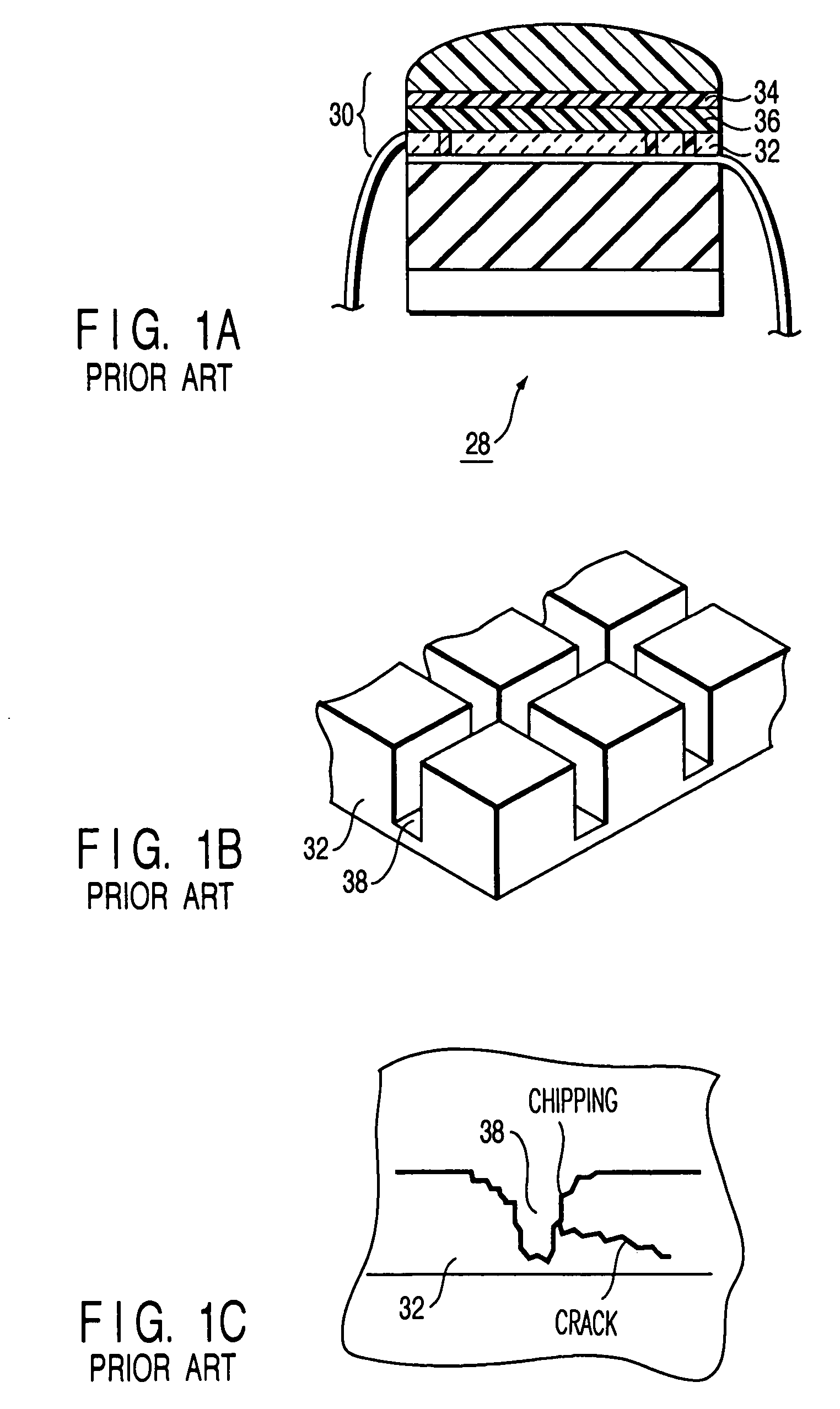
However, formation of this composite piezoelectric member 30 has a problem of an error in cutting work.
That is, solution-based piezoelectric single-crystal 32 generally has low breakdown resistance and is fragile, so a problem occurs in that chipping is caused in cutting work for forming a kerf 38 shown in FIG. 1B into an array-like shape.
This chipping causes characteristic deterioration and cracks in an element, thereby causing errors.
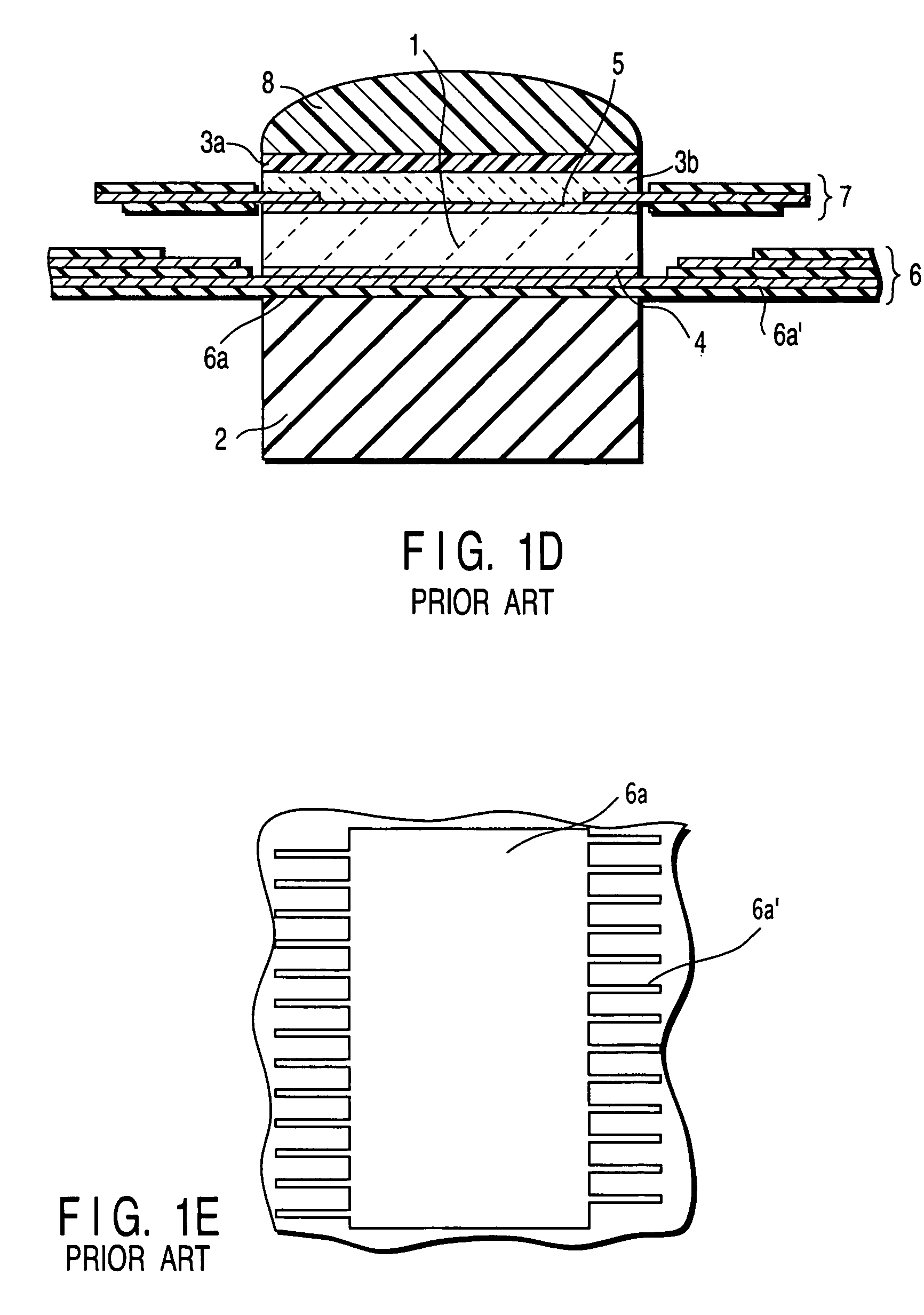
However, a problem has occurred in that cracking and chipping occur in some cases at the dicing edge part of the surface where the FPC of the single-crystal vibration element is adhered, if the above manufacturing method is adopted, a FPC whose conductive layer is extended to correspond to the area of the single-crystal vibration element is adhered to the entire surface of the vibration element by an epoxy-based adhesion, the vibration element is adhered to a backing member by an epoxy adhesion, an acoustic layer is formed on the vibration element, and array processing is thereafter carried out by a dicing saw.
In addition, burs from the conductive layer which are created during processing roughen the cutting surface of the single-crystal vibration element, and cutting wastes caught under a blade are factors which lower the cutting characteristic.
These cracking and chipping of the single-crystal vibration element are difficult to suppress even if the processing conditions are adjusted.
Large cracking causes a disconnection error and lowers the manufacturing yield while small cracking expands during use and may cause a market accident.
Also, chipping reduces the electrode area of the vibration element processed into a strip-like shape, so that not only characteristic deterioration is involved but also characteristic variants increase between array elements.

Method used


Image

  • Ultrasonic probe and method of manufacturing the same
  • Ultrasonic probe and method of manufacturing the same
  • Ultrasonic probe and method of manufacturing the same

Examples


first embodiment

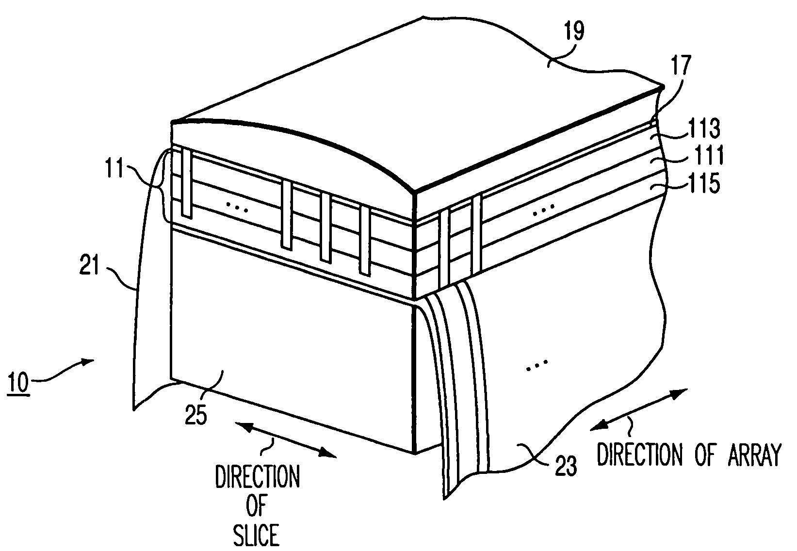
[0037]FIG. 2 shows a schematic structure of an ultrasonic probe 10 according to the first embodiment.

[0038]In FIG. 2, the ultrasonic probe 10 is constructed in a structure comprising a composite piezoelectric member (1-3 type) 11, an acoustic matching layer 17, an acoustic lens 19, a common electrode plate 21, a flexible wiring substrate 23, and a backing member 25.

[0039]The composite piezoelectric member (1-3 type) 11 includes a single-crystal piezoelectric member 111, an upper PVC resin layer 113, and a lower PVC resin layer 115. That is, the composite piezoelectric member (1-3 type) 11 is a piezoelectric member in which one-dimensional narrow rod made of single-crystal piezoelectric ceramics is embedded in a PVC resin matrix as a three-dimensional macro-molecule, and has a high electromechanical coupling factor and low acoustic impedance. Electrodes, which are not shown in the figure, for transmitting / receiving an electric signal based on a piezoelectric direct effect and a piezo...

second embodiment

[0070]In the first embodiment, explanation will be made of a method of manufacturing a 1-3 type composite piezoelectric member 11 and a method of manufacturing an ultrasonic probe 10 using the piezoelectric element. In contrast, in the second embodiment, explanation will be made of a method of manufacturing a 2-2 type composite piezoelectric member and a method of manufacturing an ultrasonic probe using the 2-2 type composite piezoelectric member.

[0071]Since the outer appearance of the ultrasonic probe using the 2-2 type composite piezoelectric member is the same as that of the ultrasonic probe 10 using the 1-3 type composite piezoelectric member shown in FIG. 3, the same figure will be also used and explanation of those components that have already been explained will be omitted herefrom. In addition, explanation of those parts that overlap the manufacturing methods explained in the first embodiment will be also omitted and only the different parts will be explained below.

[0072]The...

third embodiment

[0083]In the third embodiment, explanation will be made of a method of manufacturing a two-dimensional array type ultrasonic probe in which ultrasonic vibration elements are two-dimensionally arrayed (e.g., in a matrix-like array) with use of a 1-3 type composite piezoelectric member 11.

[0084]FIG. 4 is a lateral cross-sectional view of a two-dimensional array type ultrasonic probe 30 according to the third embodiment.

[0085]Those components that have already been explained with reference to FIG. 3 are denoted at common reference symbols and explanation thereof will be omitted herefrom. In addition, explanation of those parts that overlap the manufacturing methods described in the first and second embodiments will be omitted herefrom, and only different parts will be explained below.

[0086]In the method of manufacturing a 1-3 type composite piezoelectric member 11 according to the third embodiment, the first and second steps are the same as those of the first embodiment.

[0087]Explained...


PUM


Abstract

An ultrasonic probe is characterized in that a piezoelectric member 111 formed of solution-based single-crystal containing at least plumbum titanate is sandwiched between resin layers 113 and 115 having smaller acoustic impedance than the piezoelectric member and having conductivity, so processing errors are prevented from occurring during cutting and the resin layers can be used as acoustic layers or electrodes.

Description

CROSS-REFERENCE TO RELATED APPLICATIONS[0001]This application is based upon and claims the benefit of priority from the prior Japanese Patent Application No. 2000-029309, filed Feb. 7, 2000, the entire contents of which are incorporated herein by reference.BACKGROUND OF THE INVENTION[0002]The present invention relates to an ultrasonic probe for used in an ultrasonic diagnosis apparatus, an ultrasonic treatment apparatus, and the like, and a method of manufacturing the probe.[0003]An ultrasonic probe is constructed with a piezoelectric member used as a main member, emits an ultrasonic wave to a target object, and receives reflection waves from interfaces between which acoustic impedance differs, thereby to image the inner state of the target object. As an ultrasonic imaging apparatus which adopts this kind of ultrasonic probe, for example, there is a medical diagnosis apparatus for inspecting inside of a human body, an inspection apparatus for the purpose of flaw detection inside met...

Claims


Application Information

Patent Timeline
IPC IPC(8): A61B8/00B06B1/06G10K11/02H04R17/00
CPCB06B1/0622H01L41/37H01L41/183G10K11/02A61B8/00H01L41/338H10N30/85H10N30/852H10N30/088H10N30/092
Inventor TAKEUCHI, TAKASHIHOSONO, YASUHARUIZUMI, MAMORUYAMASHITA, YOHACHI
Owner TOSHIBA MEDICAL SYST CORP
Learn More