
Two step post-deposition treatment of ILD layer for a lower dielectric constant and improved mechanical properties

a technology of mechanical properties and dielectric constant, which is applied in the direction of cable/conductor manufacturing, semiconductor/solid-state device details, plasma technique, etc., can solve the problems of large increase in dielectric constant, degrade device performance, and etching and polishing action, so as to improve hardness and thermal stability of composite materials, reduce the dielectric constant, and improve the effect of hardness and thermal stability

Inactive Publication Date: 2007-07-31
TAIWAN SEMICON MASNUFACTURING
View PDF11 Cites 20 Cited by
  • Summary
  • Abstract
  • Description
  • Claims
  • Application Information

AI Technical Summary

Benefits of technology

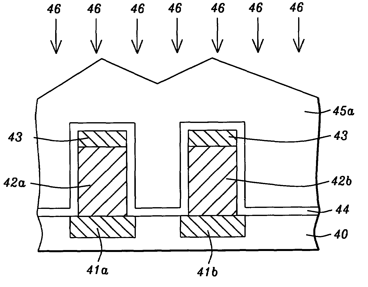
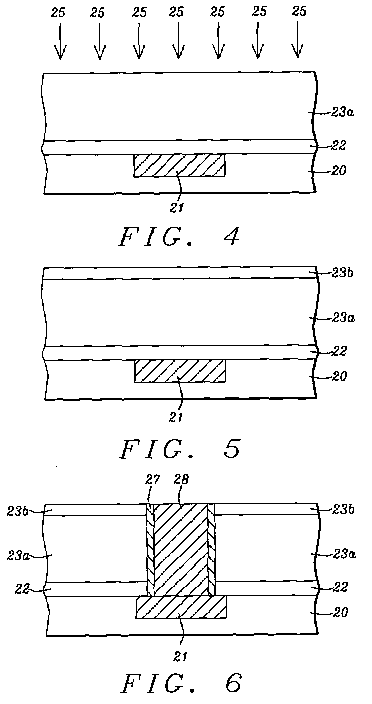
The present invention provides a method for improving the mechanical, insulating, and thermal stability of a low k dielectric layer in a semiconductor device. This is achieved by depositing a low k material on a substrate and then curing it at a high temperature to drive off water and trace amounts of monomers and solvents. The method includes a two step plasma treatment process that includes a first step with a helium plasma to promote crosslinking and a second step with a hydrogen plasma to improve thermal stability. The modified low k dielectric layer is patterned and can be used in an interconnect structure between metal lines in a semiconductor device. The resulting low k dielectric layer has a lower dielectric constant, improved mechanical stability, and better thermal stability than an untreated low k dielectric layer.

Problems solved by technology

The etching and polishing action during a CMP step is likely to scratch or form an indentation in the surface of a soft insulating material.
These surface defects will degrade device performance if not corrected by an expensive rework process.
Water uptake leads to a large increase in dielectric constant which defeats the purpose of the low k dielectric material.
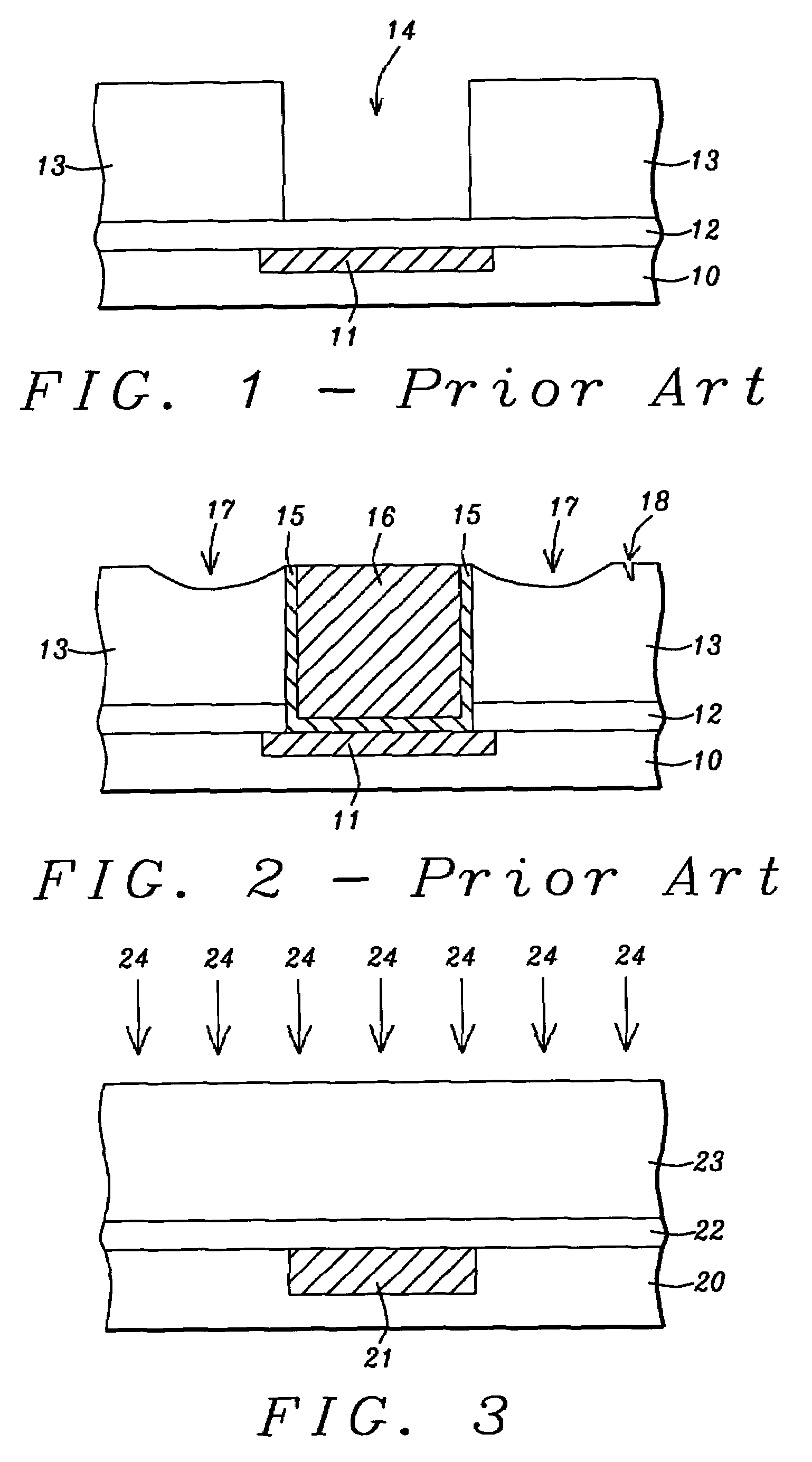
One problem associated with the damascene process is that a soft dielectric layer 13 is susceptible to the formation of defects such as a divot 17 and a scratch 18.
For example, a SiCOH layer that is not densified is likely to suffer divot and scratch defects 17, 18 that may be removed by a rework process but such an effort adds considerable expense to the fabrication scheme.
Prior art methods can prevent a dielectric constant from becoming larger by blocking water absorption but these processes do not teach how to lower a k value of a deposited film.
Unfortunately, none of the prior art methods are capable of densifying a low k dielectric layer, improving its thermal stability and reducing its dielectric constant in a single process.

Method used


Image

  • Two step post-deposition treatment of ILD layer for a lower dielectric constant and improved mechanical properties
  • Two step post-deposition treatment of ILD layer for a lower dielectric constant and improved mechanical properties
  • Two step post-deposition treatment of ILD layer for a lower dielectric constant and improved mechanical properties

Examples


example 1

[0063]This example illustrates the advantage of the present invention with regard to a further lowering of the dielectric constant in a low k dielectric layer by a post-deposition plasma treatment. A 5000 Angstrom thick SiCOH layer was deposited on several silicon wafers in a CVD process chamber using a PECVD process comprising 2,4,6,8-tetramethylcyclotetrasiloxane(TMCTS), CH4, and O2 precursors at flow rates of 6400, 1600, and 1600 sccm, respectively at 250° C. with a chamber pressure of 5 torr, and a RF power of 1000 Watts. The wafers were cured by baking at 400° C. in an oven for 60 minutes. A k value of 3.0 was observed by a measurement performed with a Hg probe as shown in Table 1. Sample 1 was obtained by subjecting a first wafer with a SiCOH layer to H2 plasma with a RF power of 900 Watts, a H2 flow rate of 1800 sccm, a chamber pressure of 5 torr, and a substrate temperature of 400° C. for 60 seconds. Sample 2 was generated in a similar fashion except that a He flow rate of 6...


PUM

PropertyMeasurementUnit
thicknessaaaaaaaaaa
thicknessaaaaaaaaaa
chamber pressureaaaaaaaaaa

Abstract

A method of lowering the dielectric constant of an organosilicon low k dielectric layer while improving the hardness and thermal stability is provided. A deposited layer of carbon doped oxide, HSQ, or MSQ is cured and treated with a He plasma which improves hardness for a subsequent CMP step and lowers the dielectric constant. There is no loss of H2O or CH4 during the He treatment. The low k dielectric layer is then treated with a H2 plasma which converts some of the Si—O and Si—CH3 bonds near the surface to Si—H bonds, thereby further lowering the dielectric constant and increasing thermal stability that improves breakdown resistance. Moisture uptake is also reduced. The method is especially useful for interconnect schemes with deep sub-micron ground rules. Surprisingly, the k value obtained from two different plasma treatments is lower than when two He treatments or two H2 treatment are performed.

Description

RELATED PATENT APPLICATION [0001]This application is related to the following Ser. No. 10 / 421,187, filing date Apr. 23, 2003; assigned to a common assignee.FIELD OF THE INVENTION[0002]The invention relates to the field of fabricating a semiconductor device and in particular to a method of improving the mechanical and insulating properties of a low k dielectric layer used to isolate metal layers in an interconnect structure.BACKGROUND OF THE INVENTION[0003]An important process during the fabrication of semiconductor devices is formation of metal interconnects that provide electrical paths between conductive layers. Metal interconnects consist of trenches that provide horizontal connections between conductive features and vias or contacts that provide vertical connections between metal layers. Metal layers are insulated from each other by a dielectric layer to prevent capacitance coupling or crosstalk between the metal wiring. Recent improvements in interlevel dielectric layer (ILD) p...

Claims


Application Information

Patent Timeline
Patent Type & Authority Patents(United States)
IPC IPC(8): H01L21/311H01L21/3105H01L21/312H01L21/316H01L21/4763H01L21/768H05H1/00H05H1/24
CPCH01L21/02126H01L21/02216H01L21/02274H01L21/02304H01L21/02321H01L21/0234H01L21/3105H01L21/3124H01L21/31633H01L21/76819H01L21/76826H01L21/76829H01L21/76835H01L21/02203H01L21/02211
Inventor CHANG, HUI-LINKO, CHUNG-CHIBAO, TIEN I.LU, YUN-CHEN
Owner TAIWAN SEMICON MASNUFACTURING
Learn More