
Method of removing contaminants from a silicon wafer after chemical-mechanical polishing operation

a technology of chemical-mechanical polishing and silicon wafers, which is applied in the direction of semiconductor/solid-state device manufacturing, basic electric elements, electric apparatus, etc., can solve the problems of large quantities of carbon-rich particles, surface defects, and the inability to clean a wafer with de-ionized water to remove all surface contaminants, so as to achieve a minimal by-product generation, less environmental toxic exhaust, and exceptional atomic cleansing

Inactive Publication Date: 2007-06-19
UNITED MICROELECTRONICS CORP
View PDF4 Cites 0 Cited by
  • Summary
  • Abstract
  • Description
  • Claims
  • Application Information

AI Technical Summary

Benefits of technology

[0014]Accordingly, one object of the present invention is to provide a method of completely removing contaminants from a silicon wafer after a chemical-mechanical polishing. The method includes applying an aqueous solution of ozone. Ozone molecules have an exceptional atomic cleansing effect and minimal by-product generation. In addition, the use of an aqueous ozone solution produces less environmentally toxic exhaust than conventional cleaning methods and ozone molecules have the capacity of neutralizing charged contaminants. Ultimately, surface contaminants are efficiently removed leading to the production of fewer surface defects and the use of fewer chemical reagents.

Problems solved by technology

However, during a chemical-mechanical polishing operation, contaminants that originate from the slurry or abrasive particles in the polishing pad may settle on the wafer surface after polishing.
However, the process frequently leads to a dishing of the surface of copper conductive lines and an exposure of the low dielectric constant material near the edges of the copper lines.
Consequently, a portion of the low dielectric constant material is likely to be polished away, generating large quantities of carbon-rich particles on the wafer surface.
In addition, because the carbon atoms within most types of neutral-to-acidic slurry have a potential opposite to that of a copper surface, the carbon-rich particles are likely to attach to the copper surface, producing surface defects.
However, cleaning a wafer with de-ionized water cannot remove all surface contaminants.
On the other hand, using an aqueous chemical solution to remove contaminants may damage the wafer surface.
Moreover, some of the contaminants may be chemically inert to the chemical ingredients in the aqueous solution.
For example, carbon-rich particles or chemical reaction by-products attached to the wafer may not be easily removed by the chemicals in the aqueous solution.
All the aforementioned conventional cleaning methods are inefficient in removing most contaminants from a silicon wafer and maintaining post CMP wafer surface properties.

Method used


Image

  • Method of removing contaminants from a silicon wafer after chemical-mechanical polishing operation
  • Method of removing contaminants from a silicon wafer after chemical-mechanical polishing operation
  • Method of removing contaminants from a silicon wafer after chemical-mechanical polishing operation

Examples


Embodiment Construction

[0022]Reference will now be made in detail to the present preferred embodiments of the invention, examples of which are illustrated in the accompanying drawings. Wherever possible, the same reference numbers are used in the drawings and the description to refer to the same or like parts.

[0023]The method of this invention is suitable for removing contaminants from a silicon wafer both during and after a chemical-mechanical polishing. A damascene process is used in the following example for illustrative purpose only. Hence, the illustration should not be regarded as a restriction to the application of this invention.

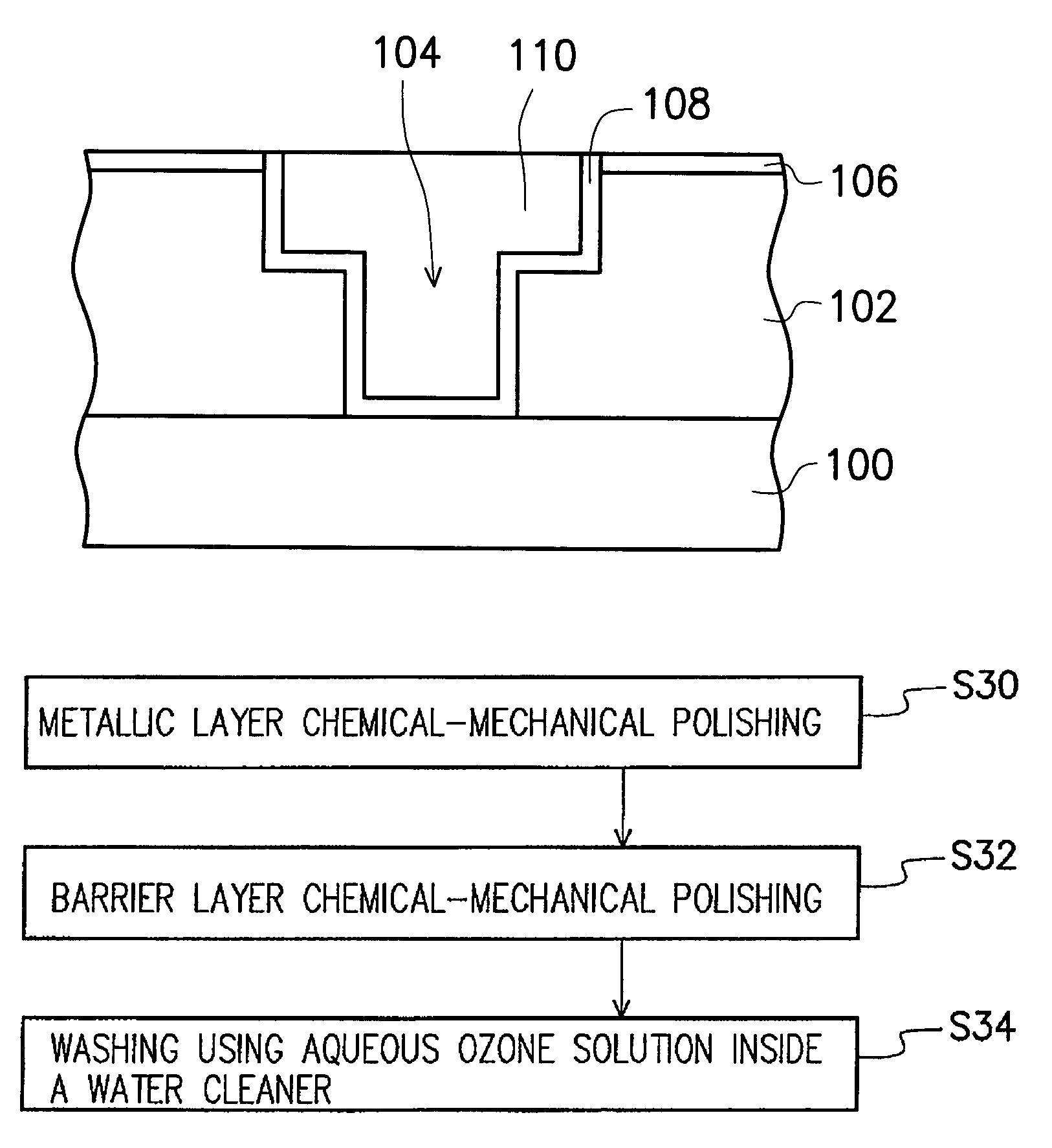
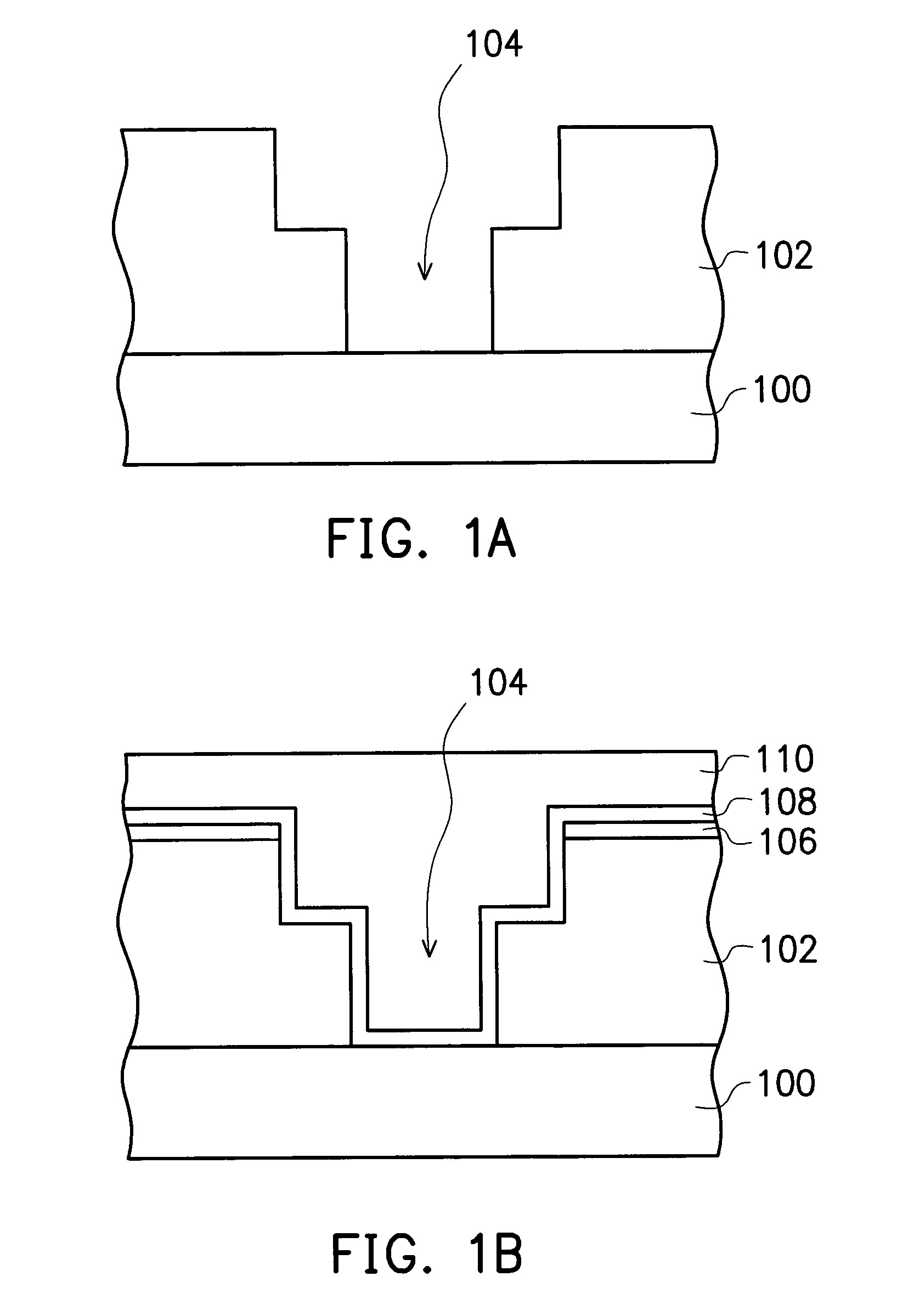
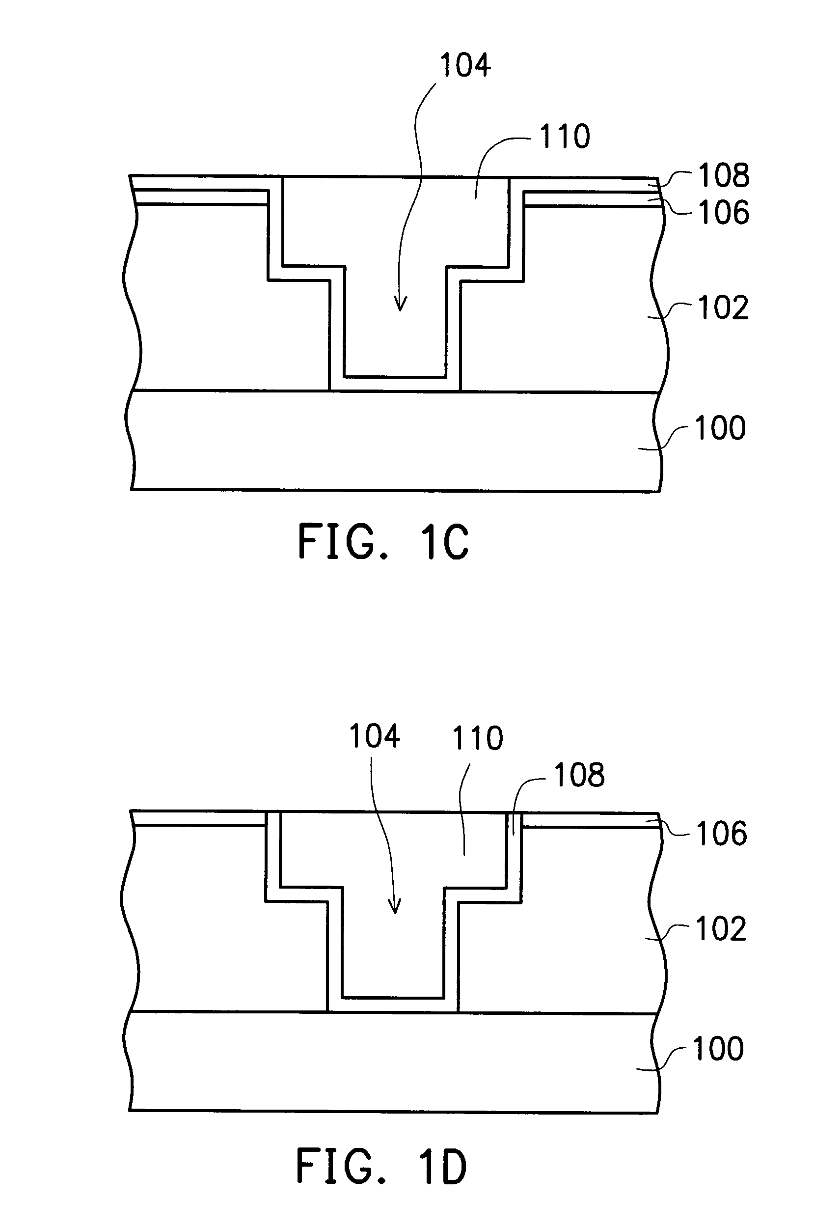
[0024]FIGS. 1A through 1D are schematic cross-sectional views showing the progression of steps for forming a damascene structure according to one preferred embodiment of this invention.

[0025]As shown in FIG. 1A, a substrate 100 (the diagram is simplified by not showing devices on the substrate 100) is provided. A dielectric layer 102 is formed over the substrate 100. The d...


PUM


Abstract

A method of removing contaminants from a silicon wafer after chemical-mechanical polishing (CMP). After a copper chemical-mechanical polishing and a subsequent barrier chemical-mechanical polishing operation, an aqueous solution of ozone in de-ionized water is applied to clean the silicon wafer so that contaminants on the wafer are removed. Alternatively, an ozone / de-ionized water buffer-polishing process is conducted after copper and barrier CMP and then the wafer is cleaned using a chemical solution or de-ionized water. Alternatively, an ozone / de-ionized water buffer-polishing process is conducted after both copper-CMP and barrier-CMP and then the wafer is cleaned using a chemical solution or de-ionized water.

Description

CROSS-REFERENCE TO RELATED APPLICATION[0001]Continuation of application Ser. No. 09 / 854,006, filed May 10, 2001 now U.S. Pat. No. 6,696,361, issued Feb. 24, 2004.[0002]This application claims the priority benefit of Taiwan application serial no. 90109738, filed on Apr. 24, 2001.BACKGROUND OF THE INVENTION[0003]1. Field of Invention[0004]The present invention relates to a planarization process in semiconductor manufacture. More particularly, the present invention relates to a post chemical-mechanical polishing (CMP) cleaning of a silicon wafer.[0005]2. Description of Related Art[0006]In the manufacturing of deep submicron semiconductors, a copper damascene process to form a conductive line in a low dielectric constant (low-k) inter-metal dielectric layer is an effective method of lowering resistor-capacitor (RC) delay and resisting electromigration resistance. In a damascene process, one important step is copper chemical-mechanical polishing (Cu-CMP) for the removal of excess copper ...

Claims


Application Information

Patent Timeline
Patent Type & Authority Patents(United States)
IPC IPC(8): H01L21/4763H01L21/302H01L21/02H01L21/306H01L21/321
CPCH01L21/02074H01L21/3212
Inventor HU, SHAO-CHUNGTSAI, TENG-CHUNHSU, CHIA-LINWEI, YUNG-TSUNG
Owner UNITED MICROELECTRONICS CORP
Learn More