
Operation analyzing method for semiconductor integrated circuit device, analyzing system used in the same, and optimization design method using the same

Inactive Publication Date: 2007-05-29
SOCIONEXT INC
View PDF7 Cites 24 Cited by
  • Summary
  • Abstract
  • Description
  • Claims
  • Application Information

AI Technical Summary

Benefits of technology

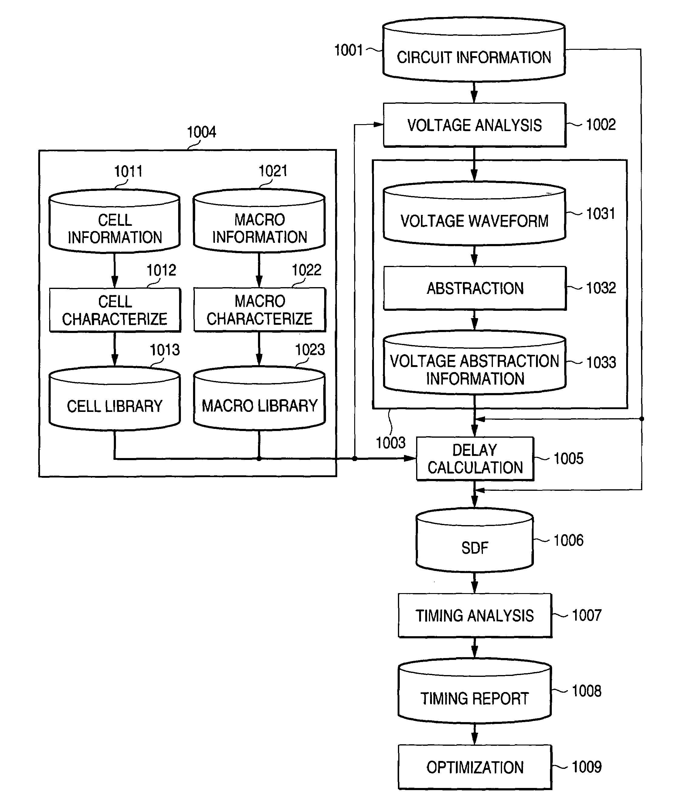
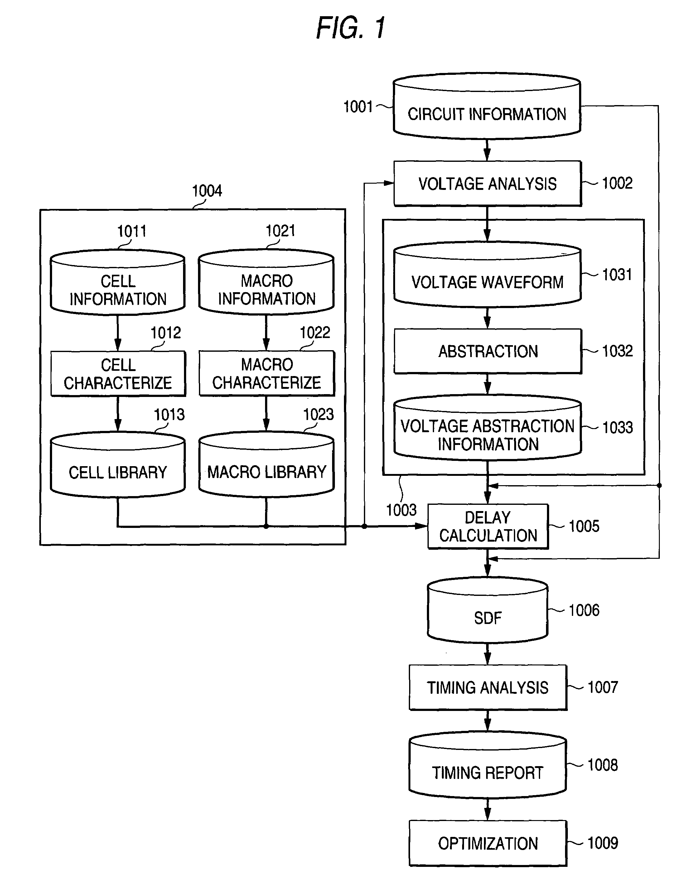
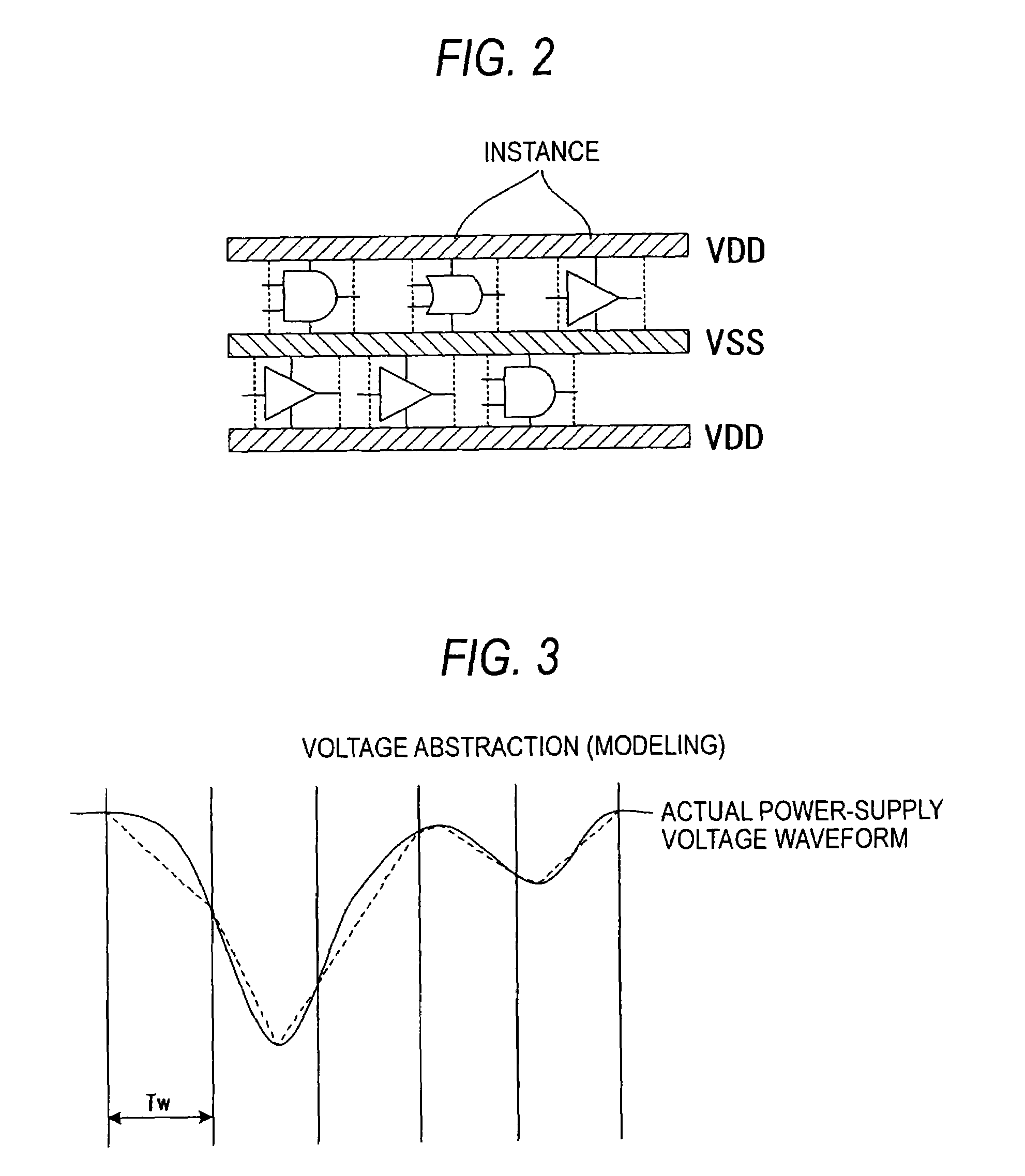
[0022]According to this configuration, the delay value is not calculated based on the average voltage, but such delay value is calculated by measuring a time and a voltage in each instance, i.e., each cell or macro of the semiconductor integrated circuit, setting the voltage obtained as dynamic data containing time data as the voltage waveform information, and abstracting the voltage waveform information. Therefore, an analyzing precision can be improved much more.
[0090]Also, if the processing step and the analyzing step are repeated until it is decided in the analyzing step that a timing difference is smaller than a predetermined value, the highly reliable processing can be executed effectively.

Problems solved by technology

For this reason, although the circuit is designed to reduce power consumption of each circuit element, a large voltage is simultaneously consumed since the number of elements is increased.
Also, a huge amount of computation is needed to execute the analysis every circuit element.
However, a delay variation of each element due to the operating voltage of each element in the circuit is not considered.
However, in the actual circuit operation, the voltage variation during the operation becomes a big problem.

Method used


Image

  • Operation analyzing method for semiconductor integrated circuit device, analyzing system used in the same, and optimization design method using the same
  • Operation analyzing method for semiconductor integrated circuit device, analyzing system used in the same, and optimization design method using the same
  • Operation analyzing method for semiconductor integrated circuit device, analyzing system used in the same, and optimization design method using the same

Examples


third embodiment

[0177]Next, a method of accelerating a delay calculation in third embodiment of the present invention will be explained hereunder. In this example, as shown in a flowchart of FIG. 7, transition times of an input signal and an output signal of the concerned cell are calculated from the circuit information to be watched, for example (calculation step 701). Then, unit windows whose input signal and output signal are translated are extracted from the abstracted information based on the transition times calculated in the calculation step 701 (extraction step 702).

[0178]Then, it is decided based on the extracted unit window whether or not the output signal is translated over the unit windows (decision step 703).

[0179]Then, if it is not decided in decision step 703 that the output signal is translated over the unit windows, the delay calculation is executed by using the previously formed library in response to the power-supply voltage (step 706).

[0180]In contrast, if it is decided in decis...

fourth embodiment

[0189]Next, a method of accelerating the delay calculation of a fourth embodiment of the present invention will be explained hereunder. In the third embodiment, the unit window is fixed. In this example, the modeling is executed by enlarging the unit window. In this example, as a flowchart is shown in FIG. 12, like the third embodiment shown in FIG. 7, transition times of the input signal and the output signal are calculated from the watched circuit information (calculation step 701). Then, the unit window containing the transition times is extracted from the abstracted information (extraction step 702). Then, if it is decide in decision step 703 that the output signal is translated over the timing windows and it is decide in decision step 704 that the power-supply voltage in the extracted unit window is different, the power-supply voltages in the unit windows associated with the transition are averaged in the third embodiment. On the contrary, in this example, an expansion of the p...

fifth embodiment

[0194]Next, data compression in the step of forming the abstract information indicated by 1003 in FIG. 1 to reduce an amount of memory use and improve the operating speed will be explained hereunder.

[0195]In this example, as shown in FIG. 15, the data are divided like meshes to hold the voltage data commonly in the same area.

[0196]A flowchart is shown in FIG. 16. A chip is divided into mesh-like areas based on circuit information (placement information) 1601, and the instances in the same area share the voltage data, as shown in FIG. 17.

[0197]Then, a representative voltage is extracted in the group, and an mean value or a center value is selected as the representative voltage (step 1632). FIG. 17A shows one mesh, and it is understood that a plurality of instances are contained in this mesh. Then, FIG. 17B is a view showing the voltage data in this mesh, wherein an axis of ordinate denotes a dropped voltage and an axis of abscissa denotes a time.

[0198]Thus, voltage abstracting inform...


PUM


Abstract

There are contained the step of forming voltage waveform information by calculating a voltage waveform of each instance of a semiconductor integrated circuit at a power-supply terminal based on circuit information and analyzing the voltage waveform of each instance, the step of forming voltage abstraction information by abstracting the voltage waveform information, and the step of calculating a delay value of the instance based on the voltage abstraction information.

Description

[0001]The present application is based on Japanese Patent Application No. 2003-164036, which is incorporated herein by reference.BACKGROUND OF THE INVENTION[0002]1. Field of the Invention[0003]The present invention relates to an operation analyzing method for a semiconductor integrated circuit device, an analyzing system used in the same, and an optimization design method using the same and, more particularly, a method of applying a high-speed and high-precision operation analysis to a large-scale and high-speed driven LSI (large-scale semiconductor integrated circuit).[0004]2. Description of the Related Art[0005]Normally, a timing analysis is important in the design of the semiconductor integrated circuit. For example, the optimization must be achieved by executing the timing analysis to decide whether or not timings among flip-flops are matched mutually. Therefore, there is employed a method that executes an optimum design of the semiconductor integrated circuit by executing a cir...

Claims


Application Information

Patent Timeline
IPC IPC(8): G06F17/50G01R31/3183G01R31/319H01L21/82H03K19/00
CPCG01R31/318357G01R31/31928G06F17/5022G06F30/33
Inventor SHIMAZAKI, KENJISATO, KAZUHIROICHINOMIYA, TAKAHIROIWANISHI, NOBUFUSAAMEKAWA, NAOKIHIRATA, MASAAKIHIRANO, SHOUZOU
Owner SOCIONEXT INC
Learn More