Semiconductor device and method for fabricating the same

a technology of semiconductor devices and electrode metals, applied in the direction of electric variable regulation, process and machine control, instruments, etc., can solve the problems of no metal having a sufficiently high work function, the lower limit of contact resistance obtained, and the work function of the electrode metal (ti) used normally, etc., to achieve high current driving ability

Active Publication Date: 2007-03-06
PANASONIC CORP
View PDF13 Cites 9 Cited by
  • Summary
  • Abstract
  • Description
  • Claims
  • Application Information

AI Technical Summary

Benefits of technology

[0016]This allows the generation of charge resulting from the different characteristics at the interfaces between the first and second semiconductor layers and thereby reduces the contact resistance in the ohmic electrode to a value lower than in a conventional semiconductor device. As a result, the current driving ability of the semiconductor device can be improved.
[0039]The method allows the fabrication of a semiconductor device having a recessed structure and functioning as a HEFT with a high current driving ability.

Problems solved by technology

However, the foregoing conventional methods for forming an ohmic contact have a problem that, when the group III nitride semiconductor forming a positive layer is of n-type, the work function of the electrode metal (Ti) used normally is not sufficiently low and the lower limit of the contact resistance obtained is defined thereby.
Another problem is that, when the nitride semiconductor forming the positive layer is of p-type, there is no metal having a sufficiently high work function and the lower limit of the contact resistance obtained is defined thereby.
The problem of the maximum carrier concentration being defined by the carrier concentration in the heavily doped nitride semiconductor layer formed between the electrode and the positive layer similarly occurs even in the case where the contact structure is applied to the source / drain electrodes of a field effect transistor.
There is also a problem that, in the step of forming the recessed structure, a normal dry etching process is low in selectivity among the nitride semiconductor layer 172 serving as the channel layer, the barrier layer 173, and the group III nitride semiconductor layer 176 which compose a multilayer structure and therefore precise control of the depth of the recess is difficult.

Method used


Image

  • Semiconductor device and method for fabricating the same
  • Semiconductor device and method for fabricating the same
  • Semiconductor device and method for fabricating the same

Examples


embodiment 1

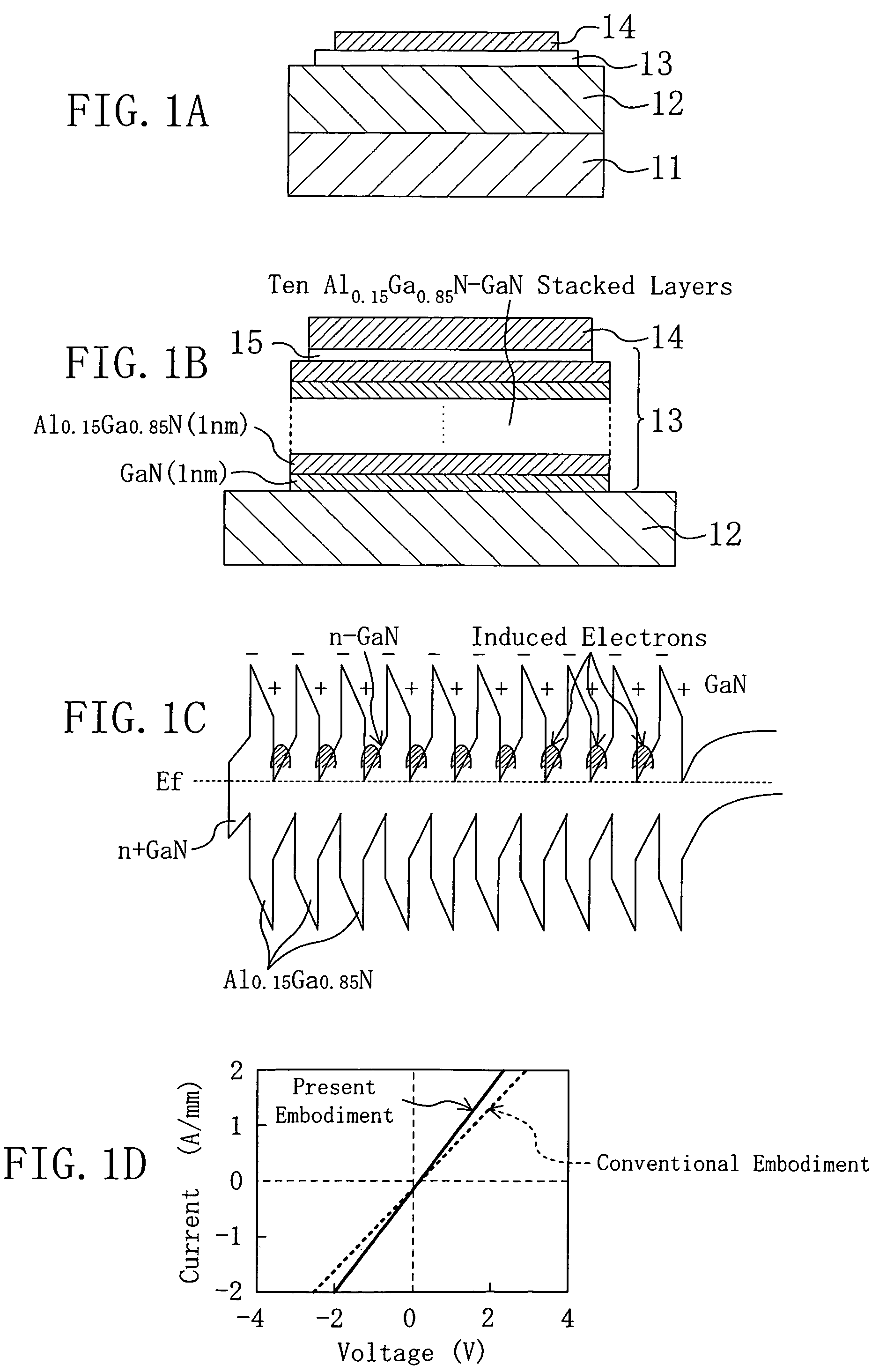
[0052]A semiconductor device in a first embodiment of the present invention will be described with reference to FIG. 1.

[0053]FIG. 1A is a cross-sectional view showing the semiconductor device according to the first embodiment. FIG. 1B is an enlarged cross-sectional view showing a structure of a multilayer film 13 in the semiconductor device of the present embodiment. FIG. 1C is an energy band diagram in a cross section of the multilayer film 13 vertical to a substrate surface. FIG. 1D is a view showing the current-voltage characteristic of each of the semiconductor device of the present embodiment and a conventional semiconductor device.

[0054]As shown in FIGS. 1A and 1B, the semiconductor device of the present embodiment comprises: a sapphire substrate 11 as a mother substrate; a semiconductor layer 12 made of a gallium nitride (GaN) with a thickness of about 2 μm which is provided on the sapphire substrate 11; a multilayer film 13 consisting of ten Al0.15Ga0.85N layers each having ...

embodiment 2

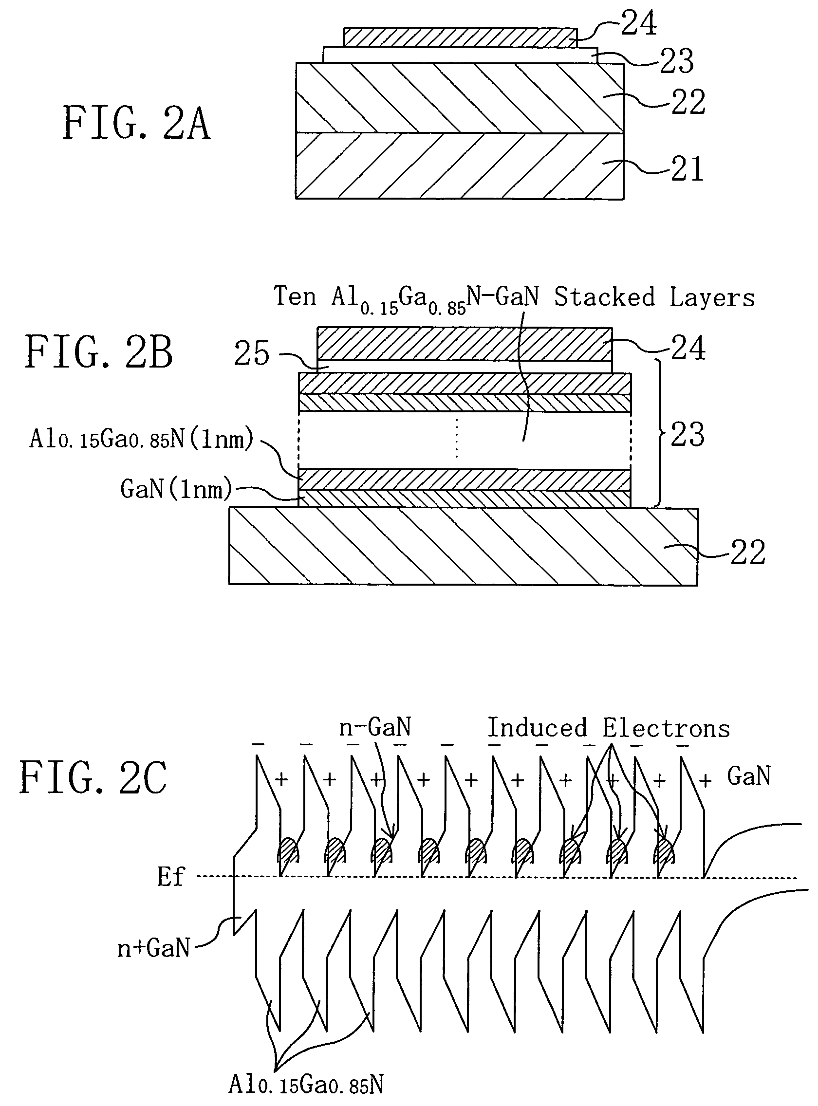
[0066]As a second embodiment of the present invention, a semiconductor device using Li smaller in work function than Ti as an electrode material will be described.

[0067]FIG. 2A is a cross-sectional view showing the semiconductor device according to the second embodiment. FIG. 2B is an enlarged cross-sectional view showing a structure of a multilayer film 23 in the semiconductor device of the present embodiment. FIG. 2C is an energy band diagram in a cross section of the multilayer film 23 vertical to a substrate surface.

[0068]As shown in FIG. 2A, the semiconductor device of the present embodiment comprises: a sapphire substrate 21; a semiconductor layer 22 serving as an active layer and made of GaN with a thickness of about 2 μm which is provided on the sapphire substrate 21; a multilayer film 23 consisting of ten Al0.15Ga0.85N layers each having a thickness of 1 nm and ten GaN layers each having a thickness of 1 nm which are alternately deposited by epitaxial growth on the semicond...

embodiment 3

[0073]As a third embodiment of the present invention, an example which uses the multilayer film described in each of the first and second embodiments in a heterojunction field effect transistor (HFET) will be described.

[0074]FIG. 3A is a cross-sectional view showing a semiconductor device according to the third embodiment. FIG. 3B is a cross-sectional view showing a conventional semiconductor device. FIG. 3C is a view showing a relationship between a drain voltage and a drain current in each of the semiconductor device of the present embodiment and the conventional semiconductor device.

[0075]As shown in FIG. 3A, the semiconductor device of the present embodiment comprises: an SiC substrate 31; a semiconductor layer 32 made of GaN with a thickness of 3 μm which is provided on the SiC substrate 31 to function as a channel layer; a barrier layer 33 made of Al0.25Ga0.75N having a thickness of 25 nm and provided on the semiconductor layer 32; a gate electrode 34 provided on the barrier l...


PUM


Abstract

A semiconductor device has a sapphire substrate, a semiconductor layer made of GaN provided on the sapphire substrate, a multilayer film provided on the semiconductor layer, and an electrode in ohmic contact with the multilayer film. The multilayer film has been formed by alternately stacking two types of semiconductor layers having different amounts of piezopolarization or different amounts of spontaneous polarization and each containing an n-type impurity so that electrons are induced at the interface between the two types of semiconductor layers. This allows the contact resistance between the electrode and the multilayer film and a parasitic resistance in a current transmission path to be reduced to values lower than in a conventional semiconductor device.

Description

[0001]The present application claims priority under 35 U.S.C. § 119(a) to Japanese Patent Applications JP 2003-165287 and JP 2004-140251, the entire contents of which are incorporated herein by reference.BACKGROUND OF THE INVENTION[0002]1. Technical Field to Which the Invention Pertains[0003]The present invention relates to a semiconductor device using a compound semiconductor and a method for fabricating the same and, more particularly, to a semiconductor device using a group III nitride semiconductor and a method for fabricating the same.[0004]2. Prior Art[0005]Because of its advantages including a wide band gap, a resultant high breakdown voltage, a high electron saturation velocity, a high mobility, and a high electron concentration in a heterojunction, the research and development of a group III nitride semiconductor have been promoted with a view to applying it to a short-wavelength light emitting element, a high-output RF element, an RF low-noise amplifier element, or the lik...

Claims


Application Information

Patent Timeline
Patent Type & Authority Patents(United States)
IPC IPC(8): H01L29/772H01L21/28H01L21/338H01L29/20H01L29/417H01L29/778H01L29/812H01L31/0328
CPCH01L29/7787H01L29/2003
Inventor HIROSE, YUTAKAUEDA, DAISUKETANAKA, TSUYOSHIUEMOTO, YASUHIROMURATA, TOMOHIRO
Owner PANASONIC CORP
Why Eureka
Try Eureka