
Damascene patterning of barrier layer metal for C4 solder bumps

a barrier layer and metal technology, applied in the field of semiconductor chip fabrication, can solve the problems of degrading the mechanical reliability of c4 solder bumps, and achieve the effects of reducing the amount of undercut, improving mechanical stability of the formed solder bump connection, and reducing the pitch

Inactive Publication Date: 2007-02-13
GLOBALFOUNDRIES INC
View PDF5 Cites 39 Cited by
  • Summary
  • Abstract
  • Description
  • Claims
  • Application Information

AI Technical Summary

Benefits of technology

The present invention provides an improved method for forming a solder bump connection at a metallic bonding pad surface of a semiconductor chip. The method includes steps of patterning a passivation layer with an opening to define a location for the solder bump connection, forming a barrier material stack including top and bottom conductive material layers conforming to the surface of the patterned passivation layer, removing a portion of the bottom conductive material layer to reduce undercut, adding a diffusion barrier layer and a solder material on the surface of the diffusion barrier layer, and removing the remaining portions of the barrier material stack. The method reduces the amount of undercut and increases the mechanical stability of the formed solder bump connection, allowing for a smaller solder bump pitch. The method also includes using a wet etching process to remove the remaining portions of the barrier material stack, which reduces the etch time and undercut. Additionally, the method includes using a patterned passivation layer with two or more via openings to improve the uniformity of solder plating.

Problems solved by technology

Unfortunately, as C4 pitch decreases, the wet etch causes increasingly more undercut of the C4 solder bump (i.e., a greater percentage of area underneath the C4 is undercut), which degrades the mechanical reliability of the C4.

Method used


Image

  • Damascene patterning of barrier layer metal for C4 solder bumps
  • Damascene patterning of barrier layer metal for C4 solder bumps
  • Damascene patterning of barrier layer metal for C4 solder bumps

Examples


Embodiment Construction

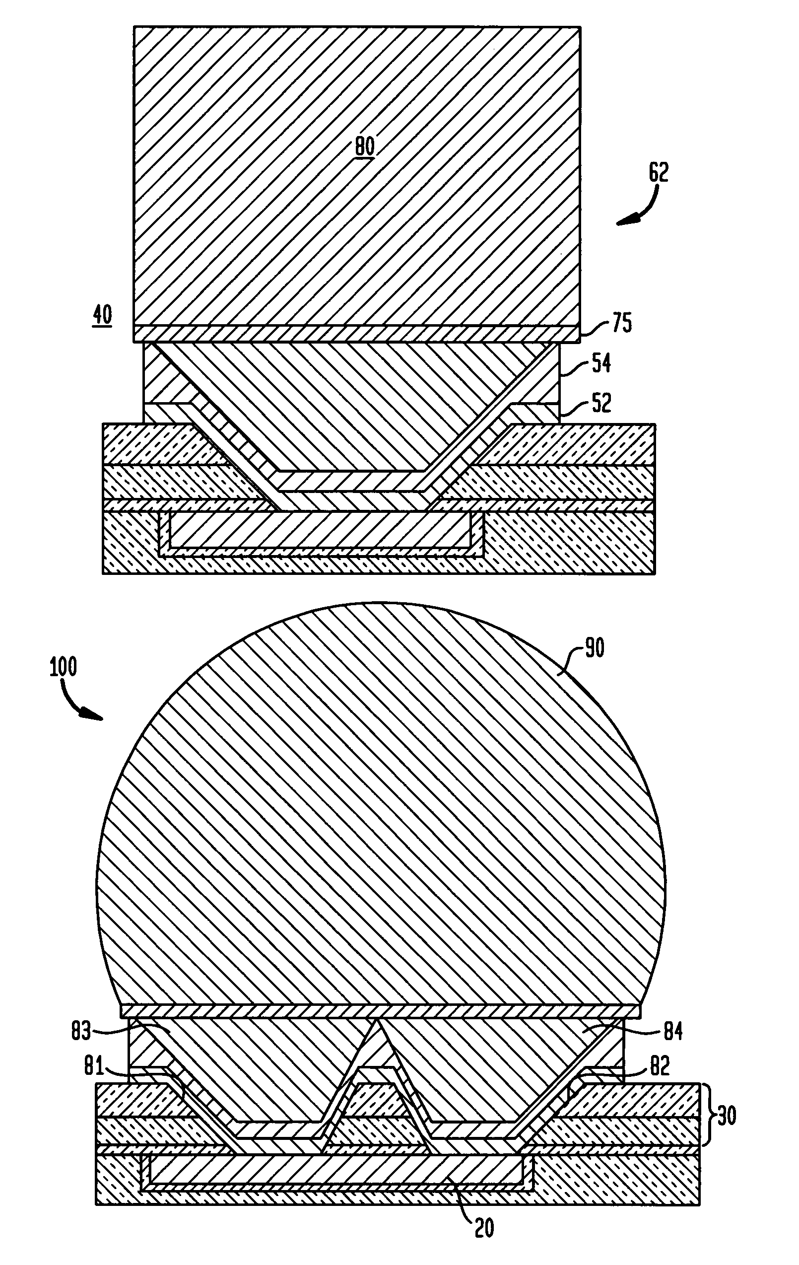
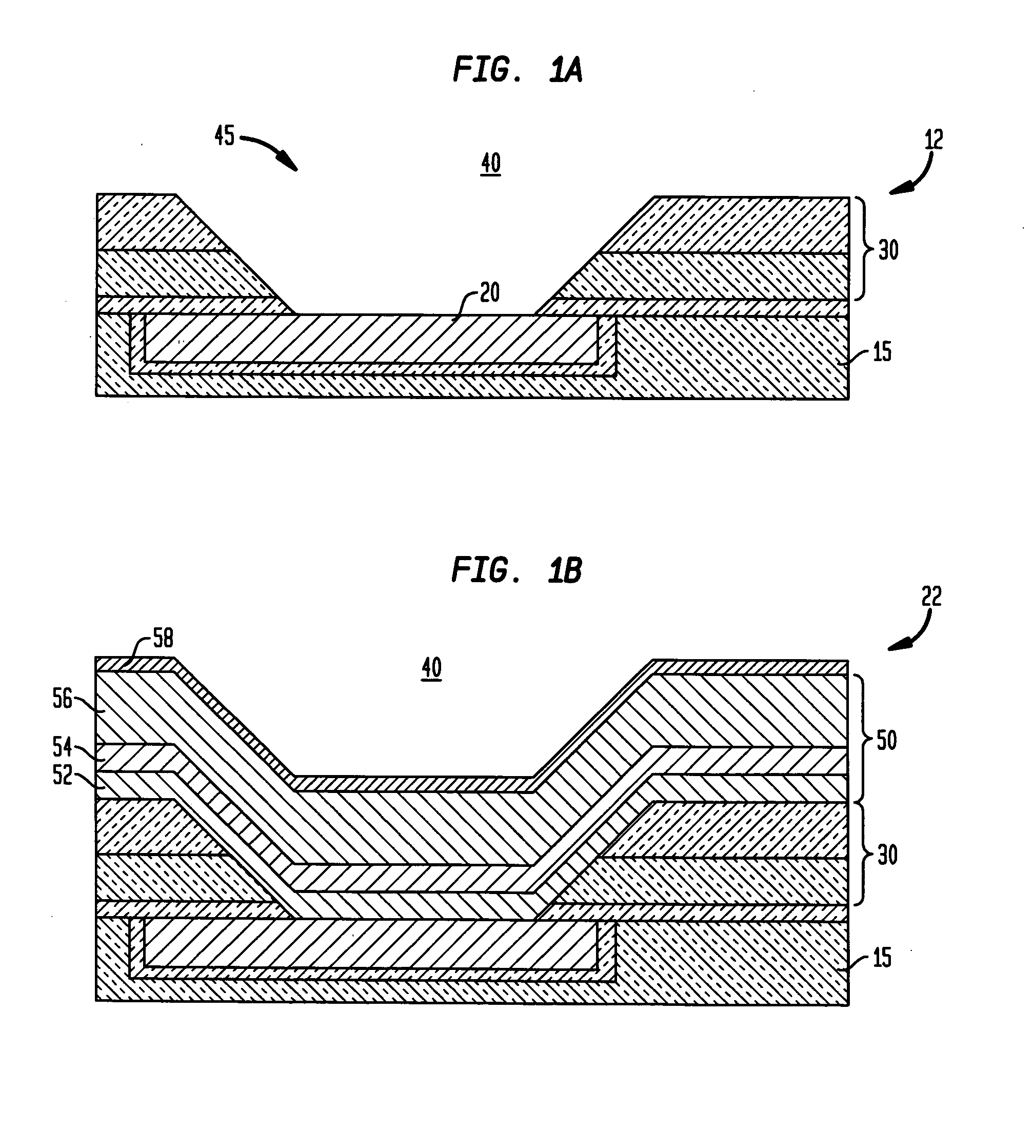
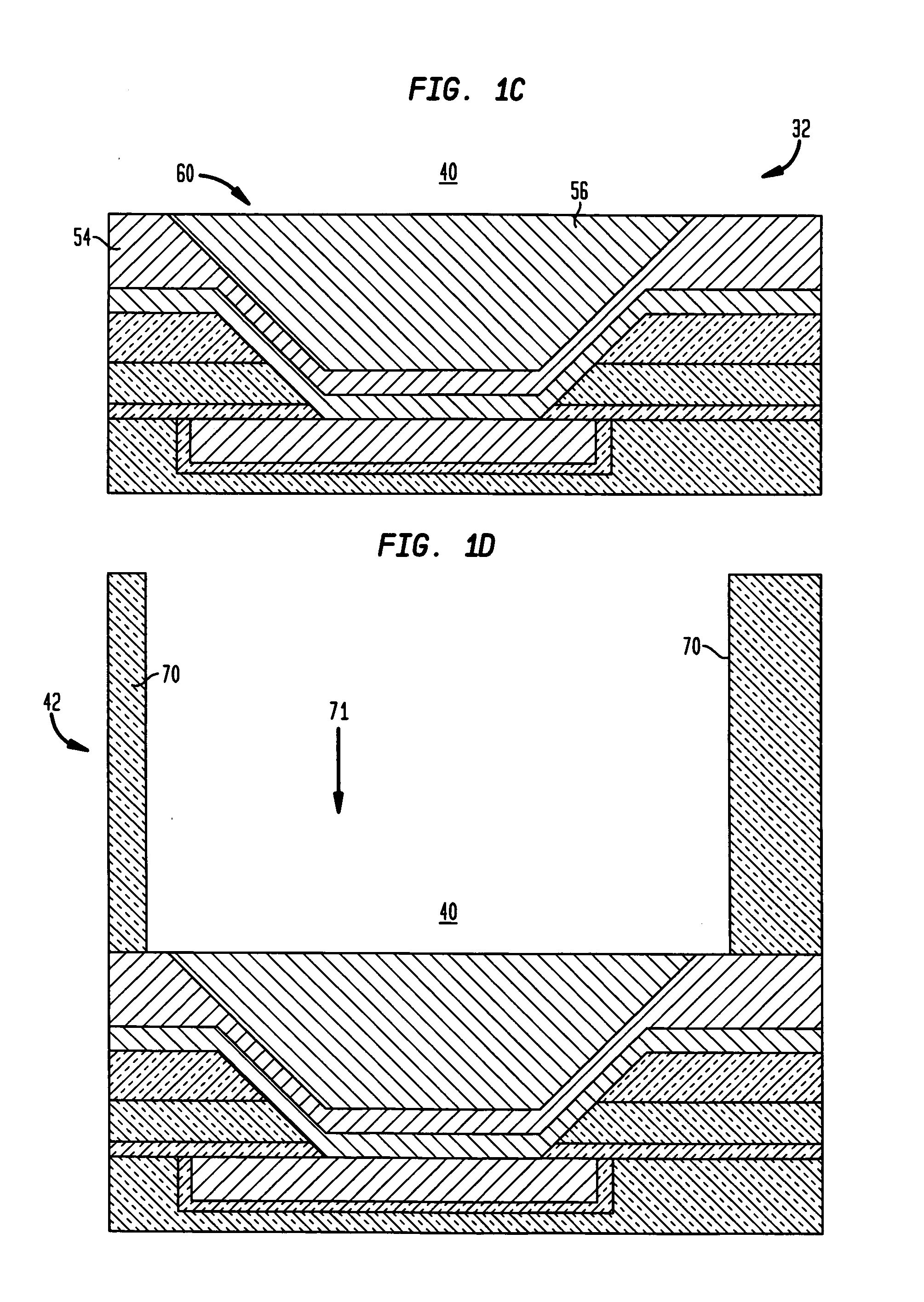
[0022]The process flow for forming a novel solder bump metallurgy according to the invention is now described with reference to FIGS. 1(a)–1(g). As shown in FIG. 1(a), a first process step 12 is depicted that includes the step of forming a passivation layer 30 upon the chip surface that includes a last conducting metal layer 20, e.g., a metallic bonding pad layer comprising Cu, Al, or other conducting metal layer, in a low-k interconnect dielectric material layer 15 such as an oxide such as FSG (i.e., fluoro-silicate glass or like fluorinated silicon oxide,) an organic dielectric, such as SiLK, or a hybrid dielectric, such as SiCOH. The passivation layer 30 is deposited using conventional deposition techniques, such as plasma-enhanced chemical vapor deposition (PECVD) and may comprise one or more passivation material layers, such as SiO2 and SiN. In one embodiment depicted in FIG. 1(a), the passivation layer 30 comprises a stack of deposited passivation material layers including a l...


PUM

PropertyMeasurementUnit
thicknessaaaaaaaaaa
thicknessaaaaaaaaaa
thicknessaaaaaaaaaa

Abstract

A system and method for forming a novel C4 solder bump for BLM (Ball Limiting Metallurgy) includes a novel damascene technique is implemented to eliminate the Cu undercut problem and improve the C4 pitch. In the process, a barrier layer metal stack is deposited above a metal pad layer. A top layer of the barrier layer metals (e.g., Cu) is patterned by CMP. Only bottom layers of the barrier metal stack are patterned by a wet etching. The wet etch time for the Cu-based metals is greatly reduced resulting in a reduced undercut. This allows the pitch of the C4 solder bumps to be reduced. An alternate method includes use of multiple vias at the solder bump terminal.

Description

BACKGROUND ART[0001]1. Field of the Invention[0002]The present invention relates generally to the fabrication of semiconductor chips, and more particularly to a structure and novel methodology for forming solder bumps in Back-End-Of-Line (BEOL) semiconductor chip processing.[0003]2. Description of the Prior Art[0004]Controlled Collapse Chip Connection (C4) processes are well known in forming solder bumps in back-end-of line semiconductor fabrication, e.g., when chips are connected to their packaging. Typically, the formation of a C4 solder bump includes the conventional formation of a metallurgical system that includes the underlying final metal layer (pad), an Under Bump Metallurgy (UBM) and the solder ball. The UBM ideally should provide good adhesion to a wafer passivation and to the IC final metal pad, and, function as an effective solder diffusion barrier.[0005]Current fabrication techniques implement Pb-free C4's using plating of the solder in a photoresist pattern, followed b...

Claims


Application Information

Patent Timeline
Patent Type & Authority Patents(United States)
IPC IPC(8): H01L23/52H01L23/40H01L23/48H01L23/485H01L23/498
CPCB23K3/0623H01L24/05H01L24/11H01L24/12H01L24/03Y10T29/49144H01L2224/0401H01L2224/05006H01L2224/05017H01L2224/05546H01L2224/05557H01L2224/05599H01L2224/11462H01L2224/1147H01L2224/11849H01L2224/11912H01L2224/13006H01L2224/131H01L2924/01005H01L2924/01013H01L2924/01014H01L2924/01015H01L2924/01022H01L2924/01028H01L2924/01029H01L2924/0105H01L2924/01073H01L2924/01074H01L2924/01078H01L2924/01079H01L2924/01082H01L2924/014H01L2924/04953H01L2924/14H01L2924/00014H01L2924/01033H01L2924/01024H01L2924/01023H01L2924/01019H01L2924/00013H01L2924/01006H01L2224/13099H01L2224/03001H01L2224/05556
Inventor DAUBENSPECK, TIMOTHY H.GAMBINO, JEFFREY P.MUZZY, CHRISTOPHER D.SAUTER, WOLFGANG
Owner GLOBALFOUNDRIES INC
Learn More