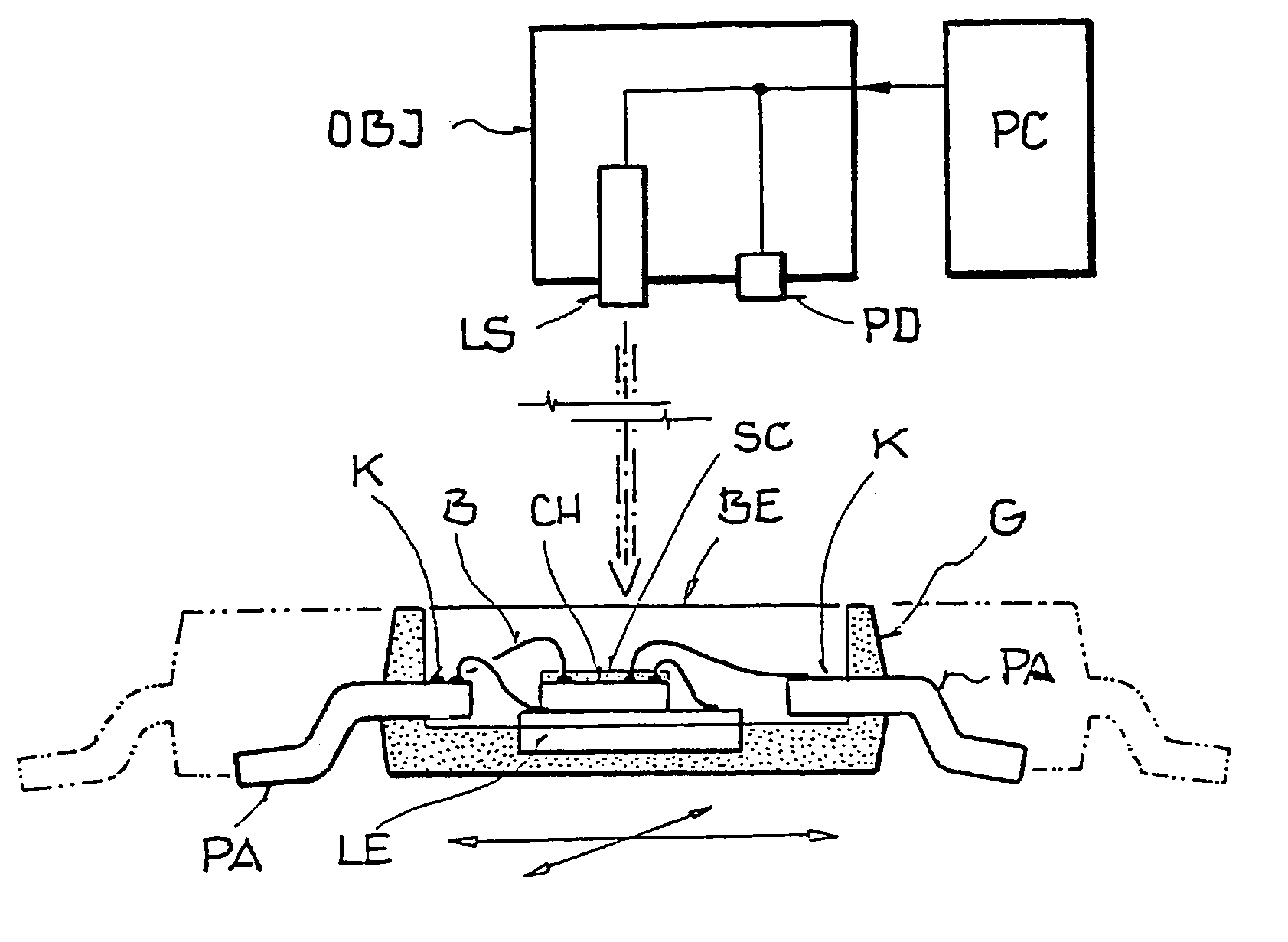
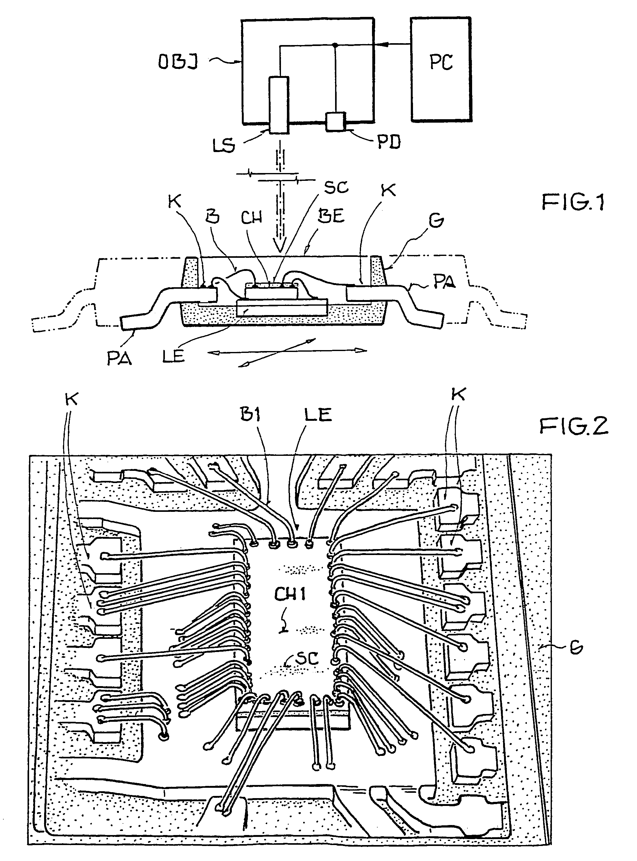
[0003]It is the object of the present invention to open the plastic housing of a potted electronic module in a manner that is automated so far as possible, and especially to avoid a destruction of an internally arranged electronic
assembly or module.
[0006]An
advantage of the method is that, with the aid of the detection of the end point, the housing of an electronic module can be opened selectively relative to the electronic module by means of a laser beam, without thereby damaging the plastic-housed electronic module and thereby unintentionally changing electrical parameters. In this context, the end point can be determined both from the analysis of the
chemical composition of the vaporizing material as well as by means of an optical measurement, for example by determination of the reflection and / or of the absorption behavior, whereby especially through the exposing of metallic contact surfaces the optical characteristics in the area to be opened are sharply or strongly changed, and the end point
signal can be especially reliably produced by means of an optical measurement. Furthermore, the reliability of the method may be increased by an over-
running time after the detection of the end point, whereby it is advantageous to reduce the power of the laser beam.
[0008]A further
advantage of the opening of the plastic housing, which comprises a protective layer, is that the electronic module is reliably protected against being damaged by means of the protective layer, in plastic housings with various different chemical compositions, especially also comprising such compounds in which other binder agents or alternative filler materials are used. In this context, the plastic of the housing is evaporated by the energy of the laser beam, whereby the potting compound comprises a high removal rate and the protective layer comprises a small removal rate, so that after a prescribed time, which is determined by means of a reference formation, the opening of the housing may be ended. Experiments of the applicant have shown that the selectivity in the removal rate between the protective layer and the potting compound is determined from the differences in the optical characteristics in the range of the laser wavelengths, the differences in the melting points, and the differences in the
evaporation temperatures. Furthermore, both a single material layer as well as a multiple-material layer, which consist of organic or inorganic compounds, can be used as the protective layer. For example,
polyimide or
siloxane as the organic protective layer, and
nitride or
oxide layers as the inorganic protective layer, as well as thin structured or patterned
metal layers can be used. In order to reduce the production costs of the protective layer, it is advantageous to integrate the application of the protective layer in the fabrication or production process of the electronic module, for example in the fabrication of an
integrated circuit. For this purpose, the protective layer is applied at the end of the fabrication process of the
integrated circuit, whereby experiments of the applicant have shown that the electronic module can be reliably protected with layer thicknesses in the range of a few microns. The method may especially be advantageously used for searching for faults or defects in potted electronic circuits. For this purpose, the potting compound
mass is removed up to (or down to) the protective layer and thereafter the conductor paths or traces are contacted without removal of the protective layer, for example at a peak measuring location, in order to test the electrical function of individual circuit blocks. A search for faults or defects is thereby considerably accelerated. Furthermore, similar housings may be opened in an automated manner, in that the process parameters of opening a preceding housing are stored in memory as a reference.
[0010]In a further development of the method, the protective layer is structured or patterned by means of a
mask step. Especially in an integration of the protective layer, which, for example, consists of
polyimide, into the production or fabrication process of an integrated circuit, it is advantageous to carry out the structuring or patterning with a contact window
mask and by means of an economical wet
chemical process. Through the removal of the protective layer in the areas of the contact windows, the protective layer may be applied before the connecting or bonding of the connecting wires (bonding). Furthermore, there is no protective layer on the contact surfaces when opening the potting compound by means of the laser. Hereby, the contact surfaces may be more easily contacted in connection with
electrical measurements.
[0012]Other experiments of applicant have shown that it is advantageous to remove rest or residues of the potting compound by a wet
chemical process step before the electrical measurement. Hereby, the contact resistances of an electrical contacting can be reduced, and existing conductive carbon compounds, which preferably only arise at high powers of the laser beam, can be removed from the surface.

