
Method of forming metal/high-k gate stacks with high mobility

a technology of high-k gate stack and high-movement metal, which is applied in the direction of semiconductor devices, electrical apparatus, transistors, etc., can solve the problems of increasing densities of electronic circuits, increasing the size of devices therein, and worrying about long-term dielectric reliability

Active Publication Date: 2006-10-03
GLOBALFOUNDRIES US INC
View PDF3 Cites 18 Cited by
  • Summary
  • Abstract
  • Description
  • Claims
  • Application Information

AI Technical Summary

Benefits of technology

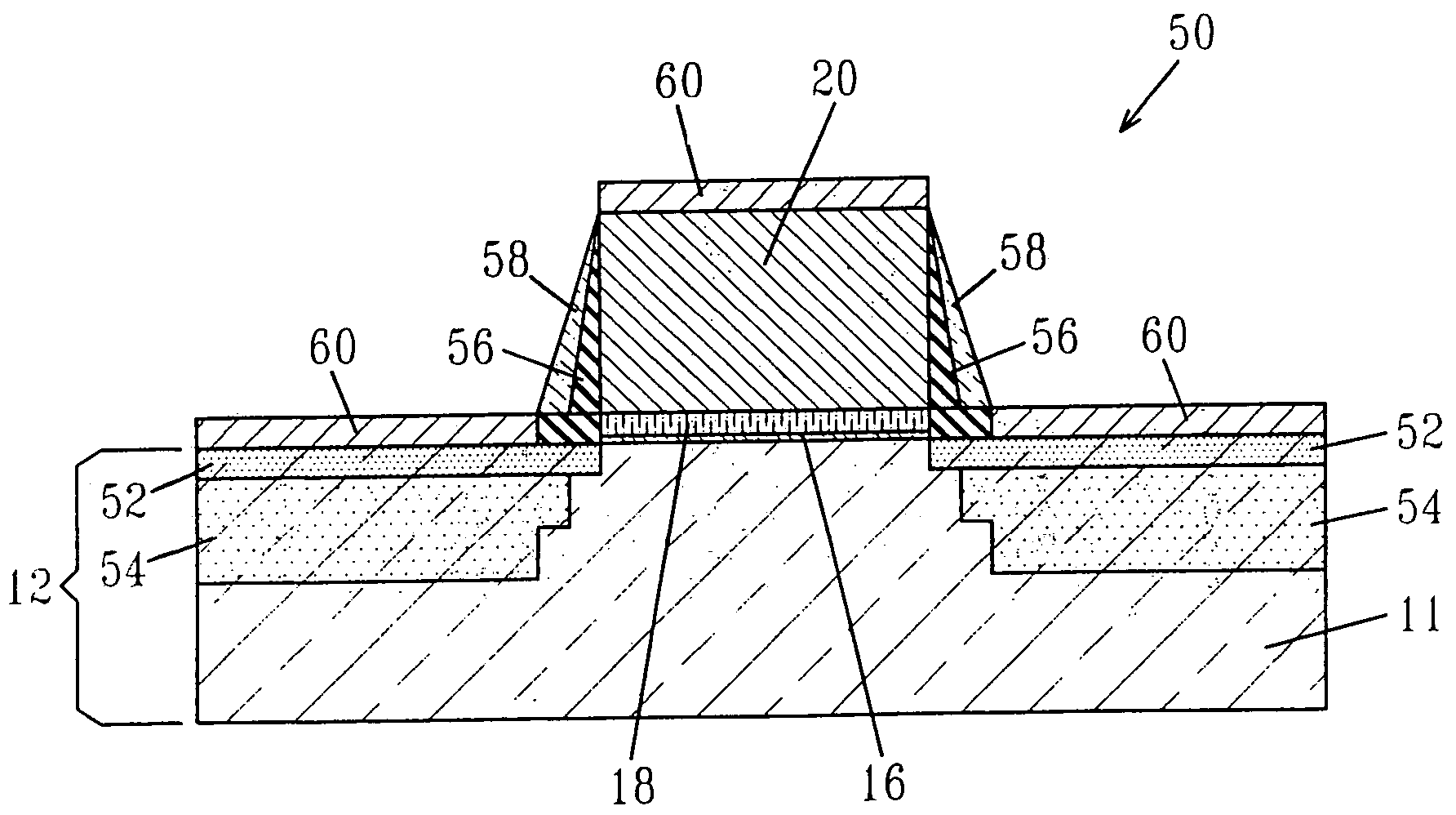
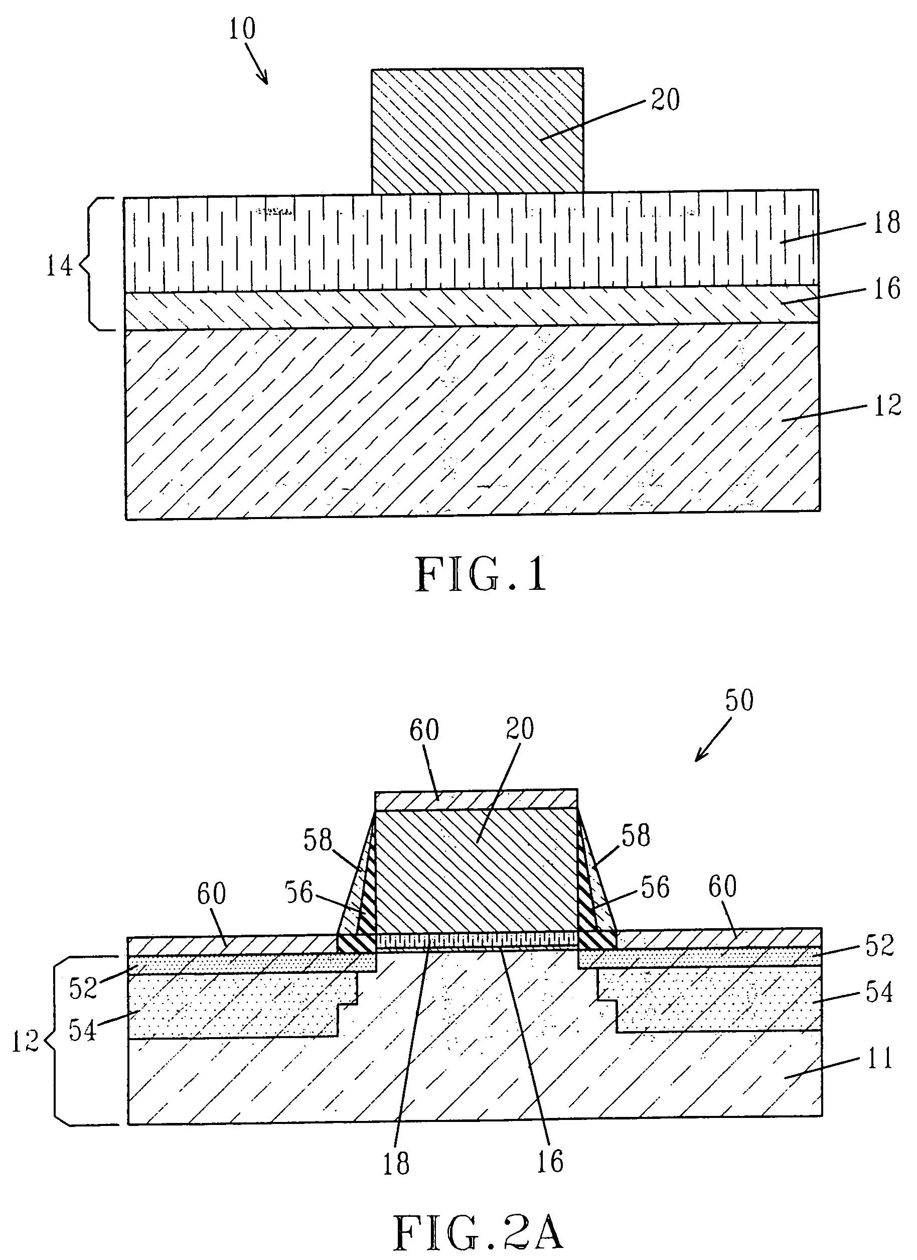
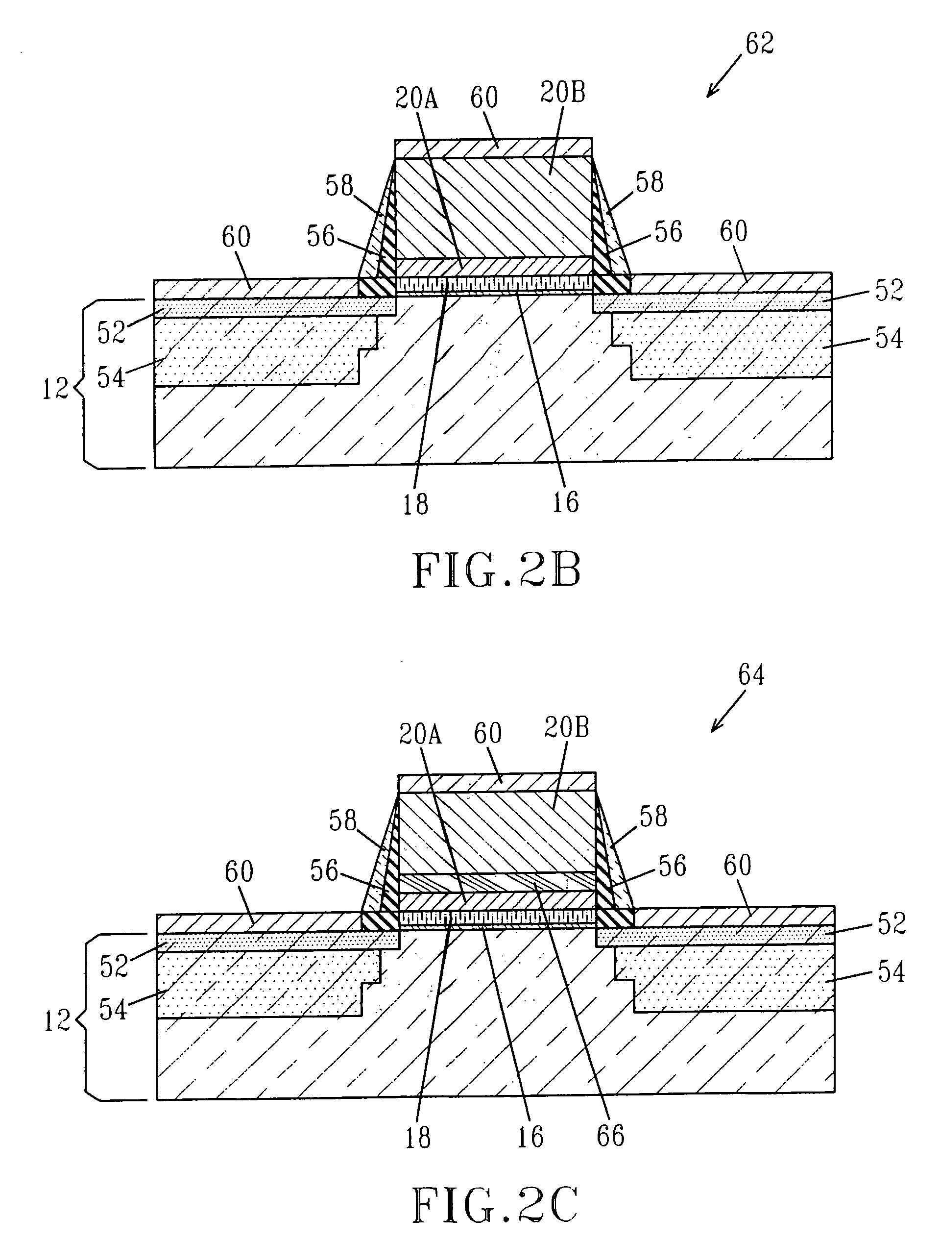
The present invention provides a gate stack structure with improved electron mobility compared to conventional metal / high-k gate stacks. The structure includes an interfacial layer with a dielectric constant greater than SiO2 and an overlaying high-k gate dielectric. The structure has an interface state density of about 8×10¹⁰ charges / cm2 or less, a peak mobility of about 250 cm2 / V-s or greater, and no substantial mobility degradation at about 6.0×10¹² inversion charges / cm2 or greater. The structure also exhibits substantially no degradation in peak mobility at electron fields of about 0.8 Mv / cm2 or greater. The semiconductor device of the present invention includes the gate stack structure and a diffusion barrier between different gate conductor materials. The method of fabricating the gate stack structure involves providing an interlayer comprising at least atoms of Si and O and an overlying high-k gate dielectric, and annealing the stack at a temperature of about 800° C or greater. The interfacial layer formed during the annealing step is different from conventional interlayers as it undergoes regrowth and intermixing with the overlaying high-k gate dielectric. The method can be integrated into conventional CMOS processing steps to provide at least one MOFFET device.

Problems solved by technology

In the quest for improved performance, electronic circuits are becoming denser and the devices therein are becoming smaller.
However as the thickness of SiO2 approaches 15 Å, substantial problems appear, including, for example, leakage currents through the gate dielectric, concerns about the long-term dielectric reliability, and the difficulty in manufacturing and thickness control.
Unfortunately, other problems have arisen from utilizing high-k dielectrics in CMOS devices including difficulty of passivating the underlying silicon, the introduction of unwanted charges in the gate stack that produce large flat band voltage shifts, large threshold voltage shifts, significant charge trapping and low electron mobility devices.
Indeed, it has been reported that the electron mobilities of metal gate electrode / high-k gate dielectric stacks formed on a silicon substrate are severely degraded when compared with conventional poysilicon / SiO2 gate stacks.
In high-k dielectrics, such as HfO2, a metal-oxygen bond is easily polarizable under an external electric field, which results in highly undesirable scattering of channel mobile charges by remote phonons present in the high-k material.
Although prior art gate stack structures (including a conventional interlayer and high-k dielectric) have reduced remote phonon scattering, they still do not achieve the electron mobility of MOS devices that contain SiO2 as the gate dielectric.

Method used


Image

  • Method of forming metal/high-k gate stacks with high mobility
  • Method of forming metal/high-k gate stacks with high mobility
  • Method of forming metal/high-k gate stacks with high mobility

Examples


example 1

[0061]This example is provided to show that the degradation in electronic mobilites within a metal-high-k gate stack can be reduced significantly when the gate stack is annealed at high temperature and an interfacial layer with a higher dielectric constant than SiO2 is formed. W / HfO2 gate stacks were formed by metal organic chemical vapor deposition (MOCVD) on thin SiO2 interfacial layers on bulk Si substrates. NMOS were fabricated by using a non-self-aligned gate process, as described by Callegari, et al., SSDM, Tokyo, Japan 2003, pp. 809–809. The gate stacks were then characterized by mobility measurements using 20×5 mm2FETs with channel doping of about 4×10¹⁷ B / cm3. Inversion charge was derived by a split CV method and drain currents were measured at Vds=30 mV.

[0062]FIG. 3 shows a set of mobility curves for a W / HfO2 gate stack as a function of increasing annealing temperature. At low annealing temperatures (less than 800° C.), mobilities were severely degraded. Electron peak mobi...

example 2

[0066]In example, a doped silicon substrate was prepared as usual for semiconductor processing. The substrate was cleaned and a thin oxide layer was grown in a liquid chemical bath containing a mixture of water, hydrogen peroxide and ammonium hydroxide which was controlled to a temperature between 20°–40° C., preferably 35° C. Subsequently, and preferably immediately, the substrate was placed into a vacuum chamber and heated to a temperature of 250°–650° C., preferably 500° C. A Hf containing metal organic precursor was delivered into the chamber and to the substrate through a showerhead. The chamber ambient may contain one or more of the following gasses: nitrogen, helium, oxygen, argon or other inert gasses preferably N2 and oxygen. The total gas pressure in the reactor was controlled to between 50 mT and 5 T, preferably 300 mT. In this fashion, a thin film consisting of hafnium oxide is grown on the substrate to between 5 and 200 Å thick (preferably 25 Å) depending on amount of t...


PUM


Abstract

The present invention provides a gate stack structure that has high mobilites and low interfacial charges as well as semiconductor devices, i.e., metal oxide semiconductor field effect transistors (MOSFETs) that include the same. In the semiconductor devices, the gate stack structure of the present invention is located between the substrate and an overlaying gate conductor. The present invention also provides a method of fabricating the inventive gate stack structure in which a high temperature annealing process (on the order of about 800° C.) is employed. The high temperature anneal used in the present invention provides a gate stack structure that has an interface state density, as measured by charge pumping, of about 8×10¹⁰ charges / cm2 or less, a peak mobility of about 250 cm2 / V-s or greater and substantially no mobility degradation at about 6.0×10¹² inversion charges / cm2 or greater.

Description

FIELD OF THE INVENTION[0001]The present invention relates to a semiconductor structure and more particularly to a gate stack structure that includes an interfacial layer comprising atoms of at least silicon and oxygen and an overlaying high-k gate dielectric. The term “high-k” is used throughout the present application to denote a dielectric material that has a dielectric constant, as measured in a vacuum, that is greater than SiO2. The gate stack structure of the present invention, which is annealed at a temperature of about 800° C. or above, has improved electron mobility and low interfacial charge density as compared to a conventional gate stack structure. Additionally, the present invention also relates to a method of forming the inventive gate stack structure. Moreover, the present invention provides a semiconductor device, i.e., metal oxide semiconductor field effect transistor (MOSFET), that includes at least the inventive gate stack structure.BACKGROUND OF THE INVENTION[0002...

Claims


Application Information

Patent Timeline
Patent Type & Authority Patents(United States)
IPC IPC(8): H01L29/76H01L29/94H01L31/062H01L31/113H01L31/119H01L21/00H01L21/28H01L21/336H01L21/84H01L29/49H01L29/51H01L29/78H01L29/786
CPCH01L21/28176H01L29/517H01L29/66575H01L29/4908H01L29/4966H01L29/513H01L29/6656H01L29/66772H01L29/7833H01L29/78684
Inventor ANDREONI, WANDACALLEGARI, ALESSANDRO C.CARTIER, EDUARD A.CURIONI, ALESSANDROD'EMIC, CHRISTOPHER P.GOUSEV, EVENGIGRIBELYUK, MICHAEL A.JAMISON, PAUL C.JAMMY, RAJARAOLACEY, DIANNE L.MCFEELY, FENTON R.NARAYANAN, VIJAYPIGNEDOLI, CARLO A.SHEPARD, JR., JOSEPH P.ZAFAR, SUFI
Owner GLOBALFOUNDRIES US INC
Learn More