
Semiconductor optical device on an indium phosphide substrate for long operating wavelengths

a technology of indium phosphide and optical devices, applied in the direction of lasers, semiconductor lasers, radiation control devices, etc., can solve the problem that the laser type is not suitable for high-temperature operation without thermal regulation, and achieve the effect of increasing the thermal performance of the laser

Active Publication Date: 2006-09-19
OCLARO NORTH AMERICA
View PDF4 Cites 14 Cited by
  • Summary
  • Abstract
  • Description
  • Claims
  • Application Information

AI Technical Summary

Benefits of technology

"The invention proposes a semiconductor optical device with a specific composition in the active layer that allows for improved performance in the C and L bands. The composition includes a small amount of nitrogen, which helps to reduce the lattice parameter of the quantum wells and obtain a state of stress in tension. The device is more efficient in converting injected electrical energy into luminous flux and requires fewer carriers for the same optical gain. The increased efficiency and reduced power consumption make it suitable for high-output applications such as lasers and optical isolators. The device also has improved stability and dynamic performance. The concentration of nitrogen can be adjusted to optimize the stress and wavelength range for different applications."

Problems solved by technology

This type of laser is not suitable for high-temperature operation without thermal regulation.

Method used


Image

  • Semiconductor optical device on an indium phosphide substrate for long operating wavelengths
  • Semiconductor optical device on an indium phosphide substrate for long operating wavelengths
  • Semiconductor optical device on an indium phosphide substrate for long operating wavelengths

Examples


example 1

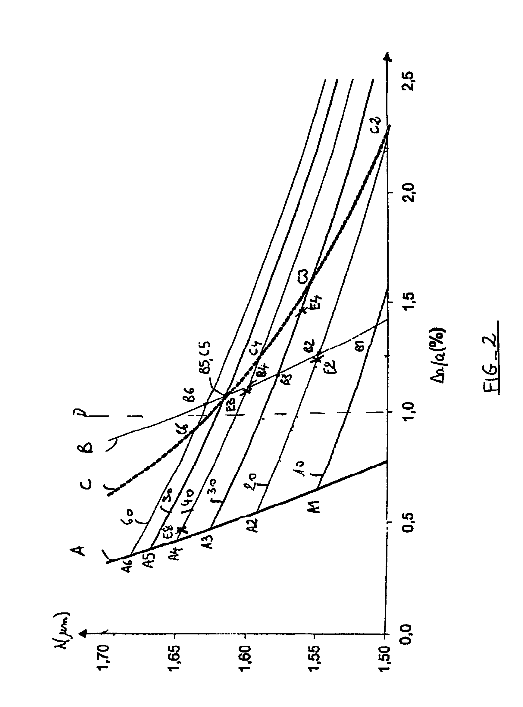
[0060]The quantum-well layer is of In0.4Ga0.6As0.995N0.005 with thickness chosen to be 14 nm for example. The operating wavelength is 1.55 μm. The quantum-well layer has a tensile stress of about 1%.

[0061]In the example the barrier layers are of Al0.31In0.69As and of thickness equal to about 10 nm.

example 2

[0062]The quantum-well layer is of In0.38Ga0.62As0.99N0.01 with thickness chosen to be 10 nm for example. The operating wavelength is 1.55 μm. The quantum-well layer has a tensile stress of about 1.25%.

[0063]In the example the barrier layers are of Al0.31In0.69As and of thickness equal to about 10 nm.

example 3

[0064]The quantum-well layer is of In0.4Ga0.6As0.99N0.01 with thickness chosen to be 14 nm for example. The operating wavelength is 1.60 μm. The quantum-well layer has a tensile stress of about 1.1%.

[0065]In the example the barrier layers are of Al0.3In0.69As and of thickness equal to about 10 nm.


PUM


Abstract

A semiconductor optical device such as a laser or semiconductor optical amplifier (SOA) based on an indium phosphide substrate or equivalent buffer layer. The active layer of the device is based on conventional InGaAs(P) alloy, but additionally includes N in order to increase the operating wavelength to greater than 1.5 μm, preferably to a wavelength lying in the C- or L-band. The active layer composition may thus be denoted In1-xGaxAsyNzPp with x≧0.48, y≦1−z−p, z≦0.05, p≧0. The active layer may include a quantum well or multi-quantum wells in which case its thickness is preferably less than the critical thickness for lattice relaxation. In other embodiments the active layer is a “massive” layer with quasi-bulk properties. The active layer may advantageously be under tensile stress, preferably roughly between 1% and 2.2%, to manipulate the light and heavy hole bands. The active layer is typically bounded by barrier layers made of a suitable semiconductor alloy, such as AlInAs or InGaAs(P).

Description

CROSS-REFERENCE TO RELATED APPLICATIONS[0001]This application claims benefit of French Patent Application No. 03 08 770, filed Jul. 18, 2003, which is herein incorporated by reference.BACKGROUND OF THE INVENTION[0002]1. Field of the Invention[0003]The present invention relates to an optical semiconductor device that has a long operating wavelength and comprises an indium phosphide substrate.[0004]2. Description of the Related Art[0005]As is well known, lasers operating at long wavelengths, i.e. above 1.5 μm, are intended to be used for optical data transmission in the so-called C band (1530–1570 nm) and / or the so-called L band (1570–1610 nm).[0006]These lasers have a vertical structure formed from a stack of semiconductor layers on a semiconductor substrate. In this stack there is an active layer, conventionally with single or multiple quantum wells separated by barrier layers, and interposed between two optical confinement layers.[0007]The document with the title “Leading-edge opto...

Claims


Application Information

Patent Timeline
Patent Type & Authority Patents(United States)
IPC IPC(8): H01L33/00H01S5/32H01S5/323H01S5/34H01S5/343
CPCB82Y20/00H01S5/3235H01S5/343H01S5/3201H01S2302/00H01S5/3403H01S5/34306H01S5/32366
Inventor GENTNER, JEAN-LOUISALEXANDRE, FRANCOISTHEDREZ, BRUNOGAUTHIER-LAFAYE, OLIVIER
Owner OCLARO NORTH AMERICA
Learn More