Light emitting device and method of manufacturing the same
a technology of light emitting devices and light emitting elements, which is applied in the manufacture of electrode systems, cold cathode manufacturing, and electric discharge tubes/lamps, etc., can solve the problems of reducing affecting the light output so as to improve the light output efficiency of the light emitting element without deteriorating the characteristics of the anode material.
- Summary
- Abstract
- Description
- Claims
- Application Information
AI Technical Summary
Benefits of technology
Problems solved by technology
Method used
Image
Examples
embodiment 1
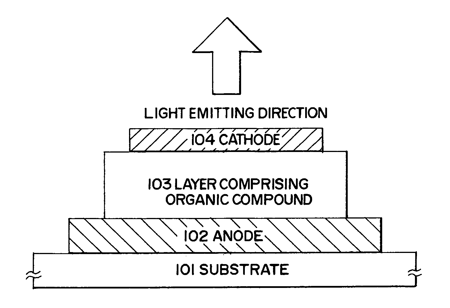
[0084]This embodiment gives a detailed description on the element structure of a light emitting element in a light emitting device of the present invention with reference to FIG. 4. Specifically, the element structure in which a low-molecular based compound is used for a layer comprising at least one organic compound will be described.
[0085]As described in Embodiment Mode, an anode 401 is formed from a light-shielding metal compound film. The anode 401 in this embodiment is an electrode electrically connected to a TFT 202 as in FIG. 3C, and is formed of TiN by sputtering to a thickness of 110 nm. Sputtering used here can be diode sputtering, ion beam sputtering, opposite target sputtering, or the like.
[0086]A layer comprising at least one organic compound 402 is formed on the anode 401. First, a hole injection layer 403 having a function of improving injection of holes from the anode is formed. The hole injection layer 403 in this embodiment is a copper phthalocyanine (Cu—Pc) film w...
embodiment 2
[0100]In this embodiment, one of the element structures of light emitting devices of the present invention is described in detail with reference to FIG. 5. Especially, the element structure formed by using high-molecular compounds to the layer comprising at least one organic compound is described.
[0101]As mentioned in Embodiment Mode, an anode 501 is formed by the metal compound film having light blocking effect.
[0102]In this embodiment, the anode 501 is connected electrically to the TFT 202 as shown in FIG. 3C, and is formed by TaN to have a thickness of 110 nm using a sputtering method. As sputtering methods used in this embodiment, two polarity sputtering method, an ion beam sputtering method, an opposite target sputtering method, or the like.
[0103]In this embodiment, a layer comprising at least one organic compound 502 formed on the anode 501 has a lamination structure constituted a hole transporting layer 503 and a light emitting layer 504. Further, the layer comprising at leas...
embodiment 3
[0114]In forming a element substrate, a method of simultaneously forming, on the same substrate, a pixel portion and TFTs (n-channel TFT and p-channel TFT) of a driver circuit formed in the periphery of the pixel portion and forming a light emitting element which is electrically connected to the TFT at pixel portion are described in detail with reference to FIGS. 6 to 9 in this embodiment. Note that, in this embodiment, light emitting element having the structure described in Embodiment Mode is formed.
[0115]First, in this embodiment, a substrate 600 is used, which is made from glass, such as barium borosilicate glass or aluminum borosilicate, represented by such as Corning #7059 glass and #1737. Note that, as the substrate 600, there is not particular limitation if the substrate is transparent to the light, even a quartz substrate can be used. A plastic substrate having heat resistance to a process temperature of this embodiment may also be used.
[0116]Then, a base film 601 formed fr...
PUM
| Property | Measurement | Unit |
|---|---|---|
| work function | aaaaa | aaaaa |
| thickness | aaaaa | aaaaa |
| thickness | aaaaa | aaaaa |
Abstract
Description
Claims
Application Information
 - R&D
- Intellectual Property
- Life Sciences
- Materials
- Tech Scout
- Unparalleled Data Quality
- Higher Quality Content
- 60% Fewer Hallucinations
Browse by: Latest US Patents, China's latest patents, Technical Efficacy Thesaurus, Application Domain, Technology Topic, Popular Technical Reports.
© 2025 PatSnap. All rights reserved.Legal|Privacy policy|Modern Slavery Act Transparency Statement|Sitemap|About US| Contact US: help@patsnap.com


