
FIB milling of copper over organic dielectrics

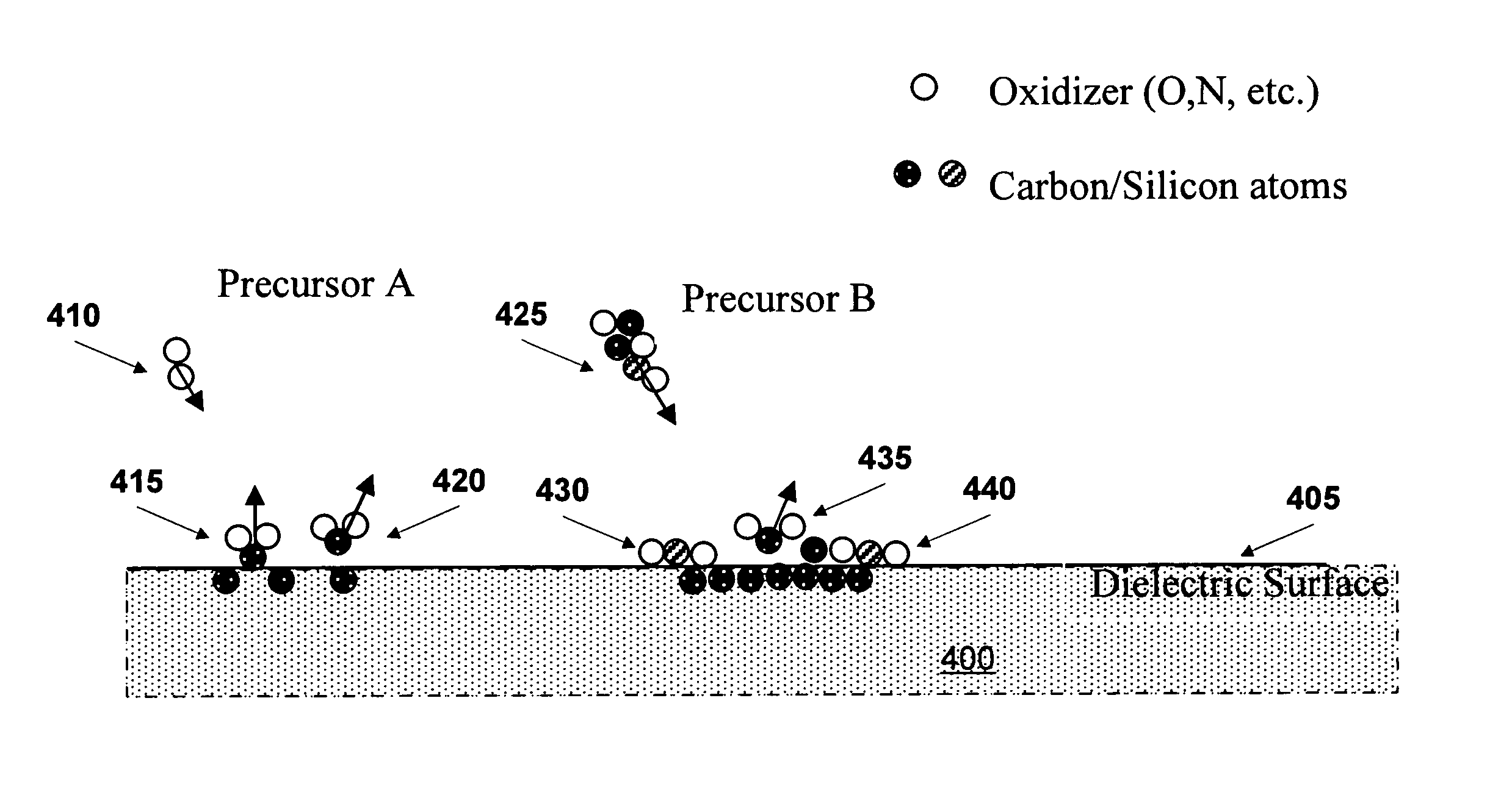
a technology of organic dielectrics and milling copper, which is applied in the field of milling copper with a focused ion beam, can solve the problems of halogen-containing compounds that are not suitable for fib milling of copper metallizations, significant damage to the underlying dielectric in exposed areas, and inability to remove residual copper, etc., to achieve the effect of improving the removal rate, high sticking coefficient and long residence tim

Active Publication Date: 2006-06-13
DCG SYST
View PDF31 Cites 22 Cited by
  • Summary
  • Abstract
  • Description
  • Claims
  • Application Information

AI Technical Summary

Problems solved by technology

This leads to significant damage to the underlying dielectric in exposed areas yet the residual copper must still be sputtered away.
But halogen-containing compounds are not suitable for FIB milling of copper metallizations.
While such compounds are effective to enhance milling, they spontaneously etch copper and corrode exposed copper within hundreds of microns from the initial beam exposure point.
Corrosion growth occurs on exposure to air of the hygroscopic copper iodides resulting from the etching process.
Corrosion of copper conductors presents serous reliability issues such as high resistivity, electrical leakage and, ultimately, conductor failure.
Many of these materials, especially organic ones, are extremely fragile under ion beam bombardment.
The current state of the art is insufficient for the challenge of copper over organic dielectric.
Precursors which are favorable for milling of copper over SiO2 are detrimental for milling of copper over organic dielectric materials.
However, this approach provides no electrical isolation benefit and, even though it enhances uniformity of milling, the application of this to FIB circuit editing is clumsy at best.
However efficient this may be for overcoming roughness formation on copper surface, it remains clumsy and at best is only a partial solution when organic low-k is involved.
But ion beam bombardment significantly changes relative contrast between grains and therefore confuses so the current density requires redefining.
In fact ion bombardment with no precursor results in the dielectric becoming conductive—carbonized.

Method used


Image

  • FIB milling of copper over organic dielectrics
  • FIB milling of copper over organic dielectrics
  • FIB milling of copper over organic dielectrics

Examples


examples

[0061]FIG. 5 is a micrograph of an unsuccessful attempt to mill copper using prior-art NH4OH as a precursor to enhance milling. Top metal layer 505 was embedded in SiO2 dielectric 510 and was successfully milled using the NH4OH precursor. An attempt to use the same regime for milling of a further copper layer 515 over organic dielectric 520 (Black Diamond™, Applied Materials Inc.) was unsuccessful as it led to unwanted exposure of a deeper metal layer 525.

[0062]FIG. 6 is a micrograph showing the same structure as in FIG. 5, but in which copper was successfully milled using Nitroethanol as precursor in accordance with an embodiment of the invention. In this example, pressure in the chamber was 1–2×10⁻⁵ Torr and the ion-beam-current density was 4 pA / μm2. As in the structure of FIG. 5, top metal layer 605 was embedded in SiO2 dielectric 610 and was successfully milled using a prior-arat process. Further copper layer 615 over organic dielectric 620 (Black Diamond™, Applied Materials Inc...


PUM

PropertyMeasurementUnit
vapor pressureaaaaaaaaaa
pressureaaaaaaaaaa

Abstract

Apparatus and processes are disclosed for milling copper adjacent to organic low-k dielectric on a substrate by directing a charged-particle beam at a portion of the copper and exposing the copper to a precursor sufficient to enhance removal of the copper relative to removal of the dielectric, wherein the precursor contains an oxidizing agent, has a high sticking coefficient and a long residence time on the copper, contains atoms of at least one of carbon and silicon in amount sufficient to stop oxidation of the dielectric, and contains no atoms of chlorine, bromine or iodine. In one embodiment, the precursor comprises at least one of the group consisting of NitroEthanol, NitroEthane, NitroPropane, NitroMethane, compounds based on silazane such as HexaMethylCycloTriSilazane, and compounds based on siloxane such as Octa-Methyl-Cyclo-Tetra-Siloxane. Products of the processes are also disclosed.

Description

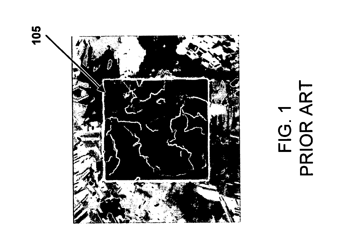
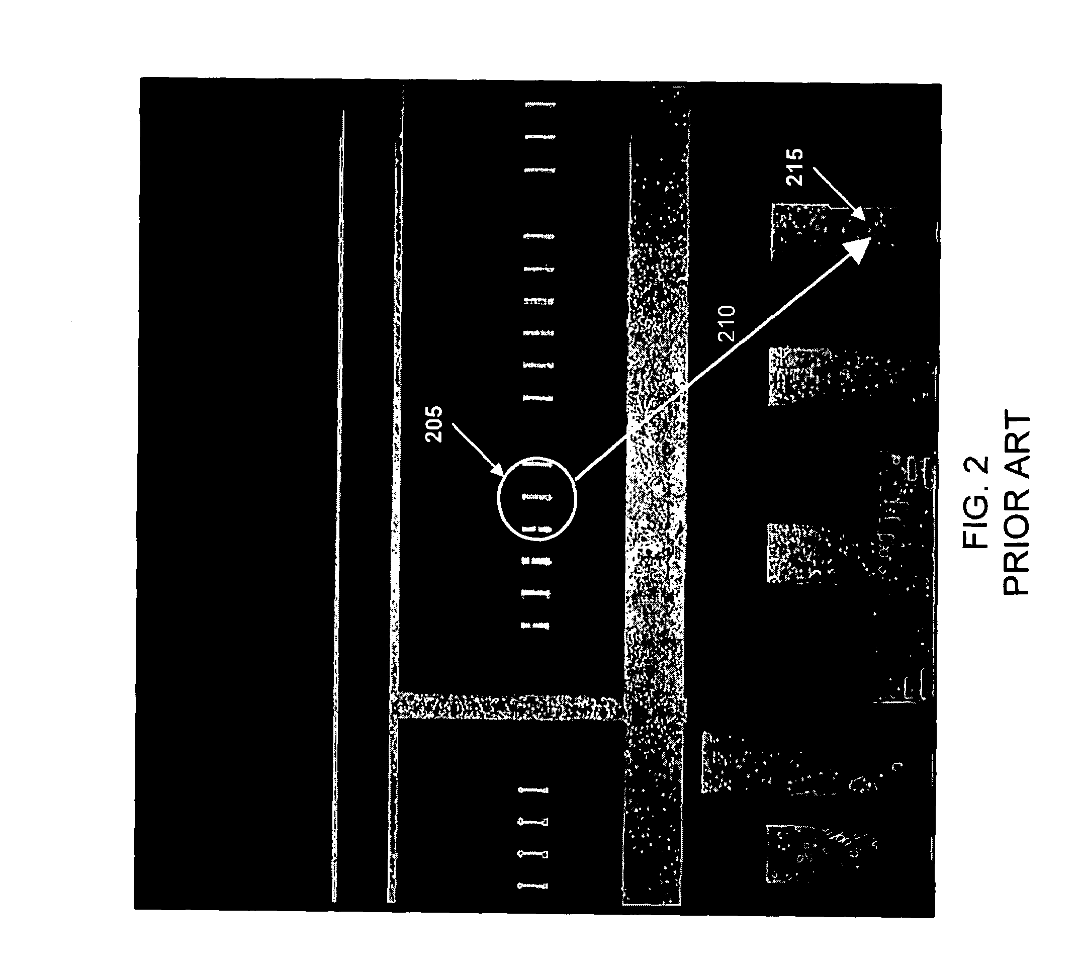
BACKGROUND OF THE INVENTION[0001]1. Field of the Invention[0002]The invention relates to milling of copper with a focused ion beam, particularly to chemically-assisted milling of copper over organic dielectric materials.[0003]2. Prior Art[0004]The primary material used for internal wiring in advanced CMOS microchips is copper. For the debugging of these microchips with a focused-ion-beam (FIB) system, copper planes and traces should be cut uniformly and cleanly so as to electrically isolate across the separation created. Normally copper planes and traces in ICs consist of crystal grains each having a specific crystallographic orientation. Different orientations show significantly different etching rates under FIB operation. As a result, FIB etching of copper leads to a strong roughness formation on the etched copper surface which then propagates, upon perforation of the copper, to the underlying dielectric. See S. HERSCHBEIN et al., The Challenges of FIB Chip Repair &Debug Assistanc...

Claims


Application Information

Patent Timeline
Patent Type & Authority Patents(United States)
IPC IPC(8): C23F1/00B44C1/22C23F4/00H01J37/305H01L21/3213
CPCC23F4/00H01J37/3053H01L21/32131H01J2237/31744H01J2237/3114
Inventor MAKAROV, VLADIMIR V.LUNDQUIST, THEODORE R.
Owner DCG SYST
Learn More