Semiconductor memory device with improved data retention characteristics

a memory device and memory technology, applied in semiconductor devices, digital storage, instruments, etc., can solve the problems of increasing chip cost, large chip size, and increasing manufacturing steps, and achieve large memory capacity, small occupancy area, and low cost

Inactive Publication Date: 2006-05-16
RENESAS ELECTRONICS CORP
View PDF11 Cites 13 Cited by
  • Summary
  • Abstract
  • Description
  • Claims
  • Application Information

AI Technical Summary

Benefits of technology

[0012]An object of the present invention is to provide a semiconductor memory device having a small occupancy area and making it possible to achieve a large memory capacity without increasing the number of manufacturing steps significantly.
[0030]Furthermore, it becomes unnecessary to use a flattening process (planarization process) step for reducing the step height between the logic and the memory. Thus, the number of the manufacturing steps can be reduced.
[0031]Additionally, by using DRAM cells as the memory cells, memory cells having a small occupancy area can be achieved. Even in the configuration in which 1-bit data is stored in two DRAM cells, the area of the memory cell unit for storing the 1-bit data can be made far smaller as compared to SRAM. Thus, a semiconductor memory device which has a small occupancy area and is suitable for merging with a logic can be achieved.
[0032]By making the word lines and the cell plate electrodes at different interconnection layers, the facing area of each of the cell plate electrodes and the corresponding storage node electrode can be made large. Consequently, the capacitance of the memory cells can be made large and a sufficiently large capacitance can be ensured against shrinking of memory cells.
[0033]By changing the cell plate voltage dependently on an operation cycle, it is possible to compensate for a change in the voltage of the storage node according to leakage current. Thus, data-holding characteristics can be improved.
[0034]By making the memory cells into the trench isolation configuration and forming the cell plate electrodes, over the insulating film, on the side walls of the trenches, the so-called isolation merged type memory cell capacitors can be realized. In memory cells subjected to shrinking, memory cell capacitors having a sufficiently large capacitance can be implemented.

Problems solved by technology

Thus, problems that the number of manufacturing steps increases significantly and chip costs increases are caused.
Thus, when an SRAM is used as a main memory having a large memory capacity, the size of the chip becomes very large.
Accordingly, it is very difficult to merge an SRAM having a memory capacity of 4 M bits or more with a logic in a system LSI having a restricted chip area.

Method used


Image

  • Semiconductor memory device with improved data retention characteristics
  • Semiconductor memory device with improved data retention characteristics
  • Semiconductor memory device with improved data retention characteristics

Examples


first embodiment

[First Embodiment]

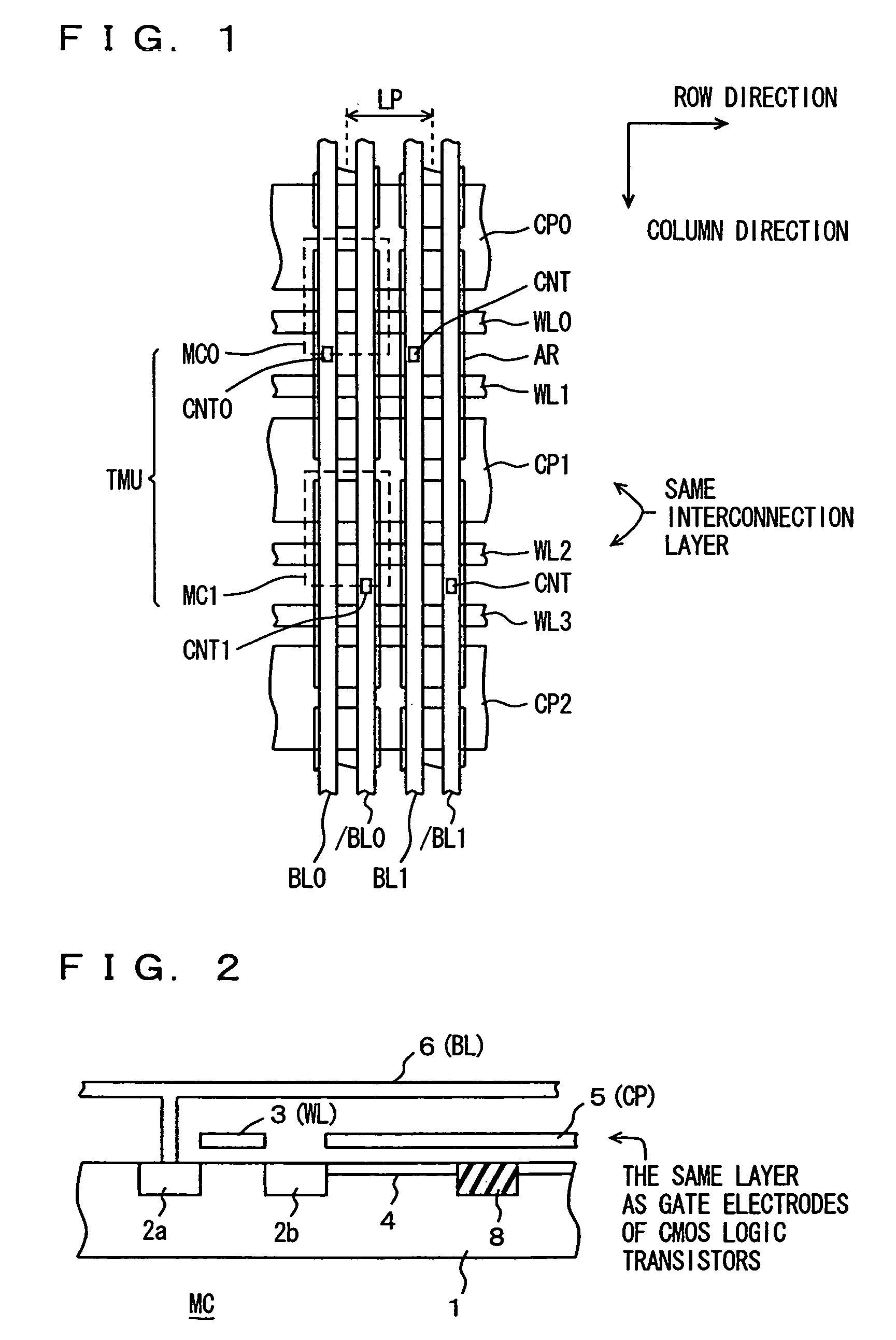
[0102]FIG. 1 is a diagram schematically showing the configuration of an array section of a semiconductor memory device according to a first embodiment of the present invention. A layout of memory cells arranged in 4 rows and 2 columns is shown representatively in FIG. 1. In FIG. 1, word lines WL0–WL3 are arranged extending in the row direction. Cell plate electrode lines CP0–CP2 are formed in the same interconnection layer as word lines WL0–WL3 and in parallel to these word lines. Accordingly, cell plate electrode lines CP0–CP2 are arranged such that adjacent cell plate lines sandwich two word lines, and are arranged extending in the row direction in the memory cell array. The cell plate electrode lines adjacent to each other in the column direction are separated from each other by a word line WL arranged in between.

[0103]Word line WL0–WL3 are arranged corresponding to memory cell rows, and are connected to the memory cells in corresponding rows.

[0104]A constant re...

third embodiment

[Third Embodiment]

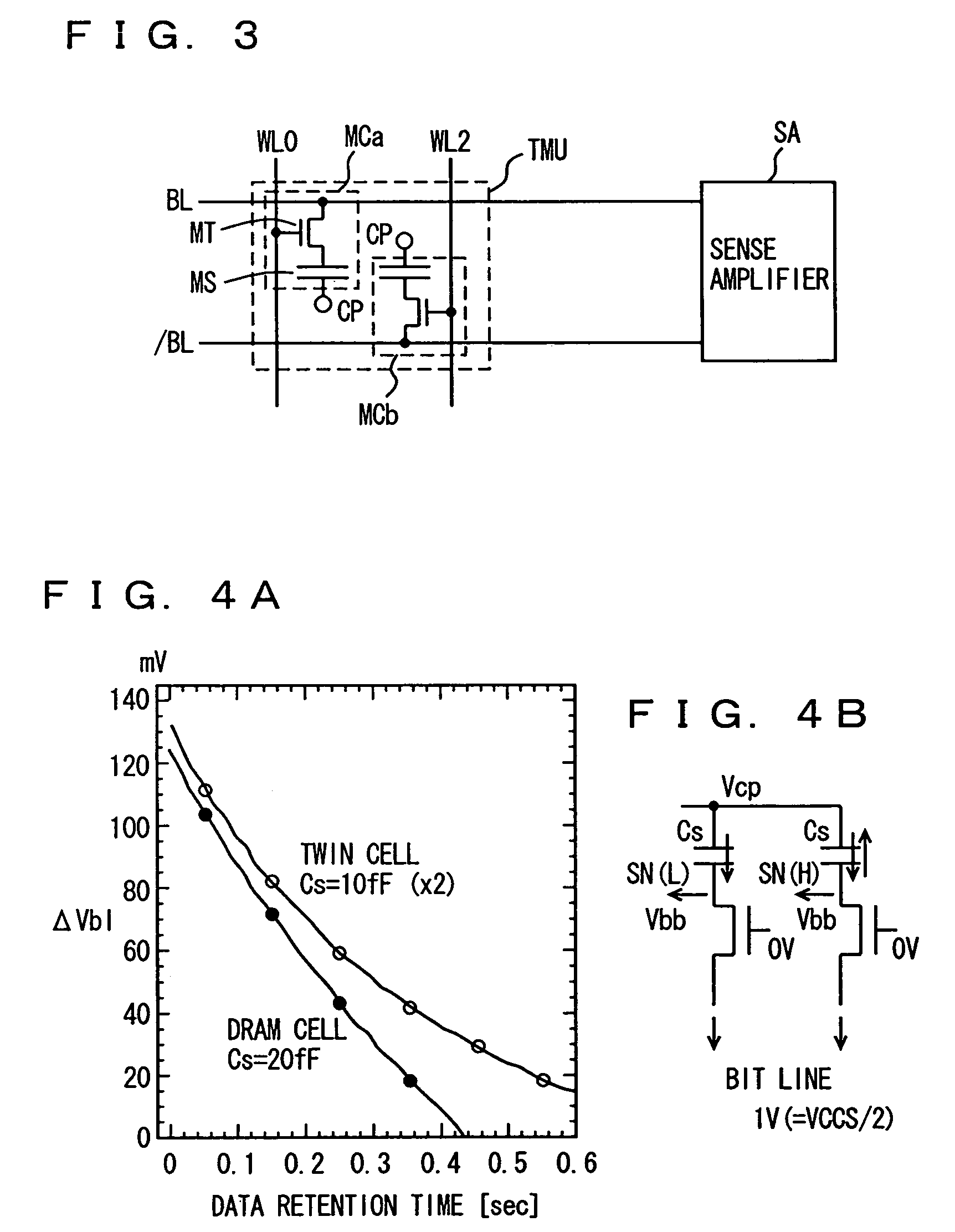
[0148]FIG. 9 is a diagram schematically showing a layout of a memory array according to a third embodiment of the present invention. The layout of memory cells illustrated in FIG. 9 is the same as the layout of the memory array illustrated in FIG. 7. In the configuration illustrated in FIG. 9, adjacent bit lines do not constitute a bit line pair. A bit line pair is provided by two bit lines with one bit line interposed in between. Upon selection of a word, one of word lines is selected. Therefore, memory cells MC0 and MC3 constitute a twin cell unit TMU, and memory cells MC1 and MC4 constitute another twin cell unit. The other configurations are the same as in FIG. 7. The same reference numerals are allotted to the corresponding components, and detailed explanation thereof is omitted.

[0149]In the configuration as illustrated in FIG. 9, one of the word lines is selected, but two word lines do not need to be selected. Thus, current consumption can be reduced.

[0150]A ...

modification example

[Modification Example]

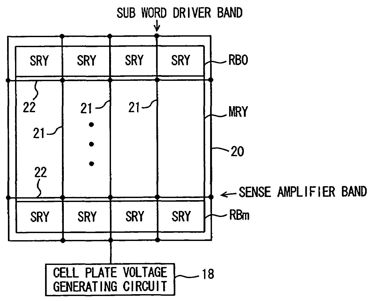
[0224]FIG. 23 is a diagram schematically showing the configuration of a modification of the third embodiment of the present invention. In FIG. 23, a bank A sense amplifier band SABA is arranged at one side, in the column direction, of a row block RBA, and a bank B sense amplifier SABB is arranged between row blocks RBA and RBB. Memory cells arranged at the crossing of a bit line pair BLPa and a sub word line SWLA in row block RBA are connected to a sense amplifier in bank A sense amplifier band SABA. On the other hand, in row block RBA, data in memory cells arranged corresponding to the crossing of a sub word line SWLB and a bit line pair BLPb are sensed and amplified by bank B sense amplifier band SABB.

[0225]A local control circuit 85 is provided to bank A sense amplifier band SABA, and a local control circuit 86 is provided to bank B sense amplifier band SABB. A latch bank designating signal BSLTA and a latch block selecting signal BSA specifying memory block...


PUM


Abstract

Conductive lines constituting word lines of memory cells and conductive lines constituting memory cell plate electrodes are formed in the same interconnecting layer in a memory device including a plurality of memory cells each including a capacitor for storing data in an electrical charge form. By forming the capacitors of the memory cells into a planar capacitor configuration, a step due to the capacitors is removed. Thus, a dynamic semiconductor memory device can be formed through CMOS process, and a dynamic semiconductor memory device suitable for merging with logic is achieved. Data of 1 bit is stored by two memory cells, and data can be reliably stored even if the capacitance value of the memory cell is reduced due to the planar type capacitor.

Description

[0001]This application is a continuation of Application Ser. No. 10 / 119,094 filed Apr. 10, 2002 now U.S. Pat. No. 6.785,157.BACKGROUND OF THE INVENTION[0002]1. Field of the Invention[0003]The present invention relates to a semiconductor memory device, and particularly to a semiconductor memory device having memory cells storing data in capacitors.[0004]2. Description of the Background Art[0005]In a data processing field and the like, a circuit device called a system LSI (large-scale integrated circuit), wherein a memory device and a logic such as a processor are integrated in the same semiconductor chip, has been widely used in order to process data at a high speed with low power consumption. In the system LSI, the logic and the memory device are interconnected through on-chip interconnect lines. Therefore, the system LSI has the following advantages: (1) since the load of the signal interconnection lines is smaller than that of on-board interconnection lines, data / signals can be tr...

Claims


Application Information

Patent Timeline
Patent Type & Authority Patents(United States)
IPC IPC(8): G11C11/24G11C11/401G11C11/404G11C11/405G11C11/407G11C11/409G11C11/4097H01L21/8242H01L27/10H01L27/108
CPCG11C7/18G11C8/14G11C11/4085G11C11/4087G11C11/4097H01L27/108H01L27/10882H01L27/0207G11C2211/4013H01L27/1085H01L27/10873H10B12/00H10B12/03H10B12/05H10B12/48
Inventor ARIMOTO, KAZUTAMISHIMANO, HIROKI
Owner RENESAS ELECTRONICS CORP
Why Eureka
Try Eureka