Method of manufacturing semiconductor device

a manufacturing method and semiconductor technology, applied in the field of semiconductor device manufacturing, can solve the problems of wiring breakdown, difficult to secure a region of sufficient width, and insufficient phase shift effect, so as to avoid narrowing of wiring width, the gate length can be shortened

Inactive Publication Date: 2005-11-29
FUJITSU SEMICON LTD
View PDF4 Cites 13 Cited by
  • Summary
  • Abstract
  • Description
  • Claims
  • Application Information

AI Technical Summary

Benefits of technology

[0017]The present invention has been made in view of the above disadvantage, and aims at providing a method of manufacturing a semiconductor device in which gate length can be shortened while avoiding narrowing of the width of wirings.

Problems solved by technology

This is because when size of the shifter pattern is not equal to or more than a predetermined value, the contrast is lowered so that effect of the phase shift cannot be sufficiently obtained.
However, due to recent rapid miniaturization of the device, it becomes difficult to secure a region of sufficient width.
Especially, a portion having a great influence due to being incapable of securing the region for the shifter pattern is wiring formed in the same layer as the layer having the gate electrode therein.
Further when two gate electrodes are disposed sandwiching wiring therebetween, the wiring may break down sometimes. Therefore, it is quite difficult to use a shifter pattern having enough width.
However, as the recent miniaturization of patterns and pitches advances, it sometimes happens that a pattern with a desired size cannot be formed when the phase edge technology is used alone.
In such a case, a trimming technology has been sometimes used together with the phase edge technology, but it still has a disadvantage that width of the wiring becomes narrower than the design value due to adoption of the trimming technology.
However, even when the resistance of the wiring is reduced by such a method, it becomes impossible to obtain the predetermined characteristics if the wiring gets narrower than the design value, especially when the wiring is long.
As a result, even when the operational speed of a transistor is increased through shortening of the gate length, performance of the semiconductor device cannot be improved sufficiently because of deterioration of the performance caused by the wiring.
Such a disadvantage has not been solved even with the method disclosed in the above-described publication.
Though it is possible to avoid merely lowering of the propagation speed of the signal by simply making the wiring pattern intentionally broader at the step of designing, it is quite difficult in a semiconductor device in which miniaturization of pitches is going on to design only the wiring broader than a predetermined value in advance.
As described above, conventionally, formation of a fine gate electrode using the phase edge technology together with the trimming technology has been extremely difficult.

Method used


Image

  • Method of manufacturing semiconductor device
  • Method of manufacturing semiconductor device
  • Method of manufacturing semiconductor device

Examples


first embodiment -

[0044]-First Embodiment-

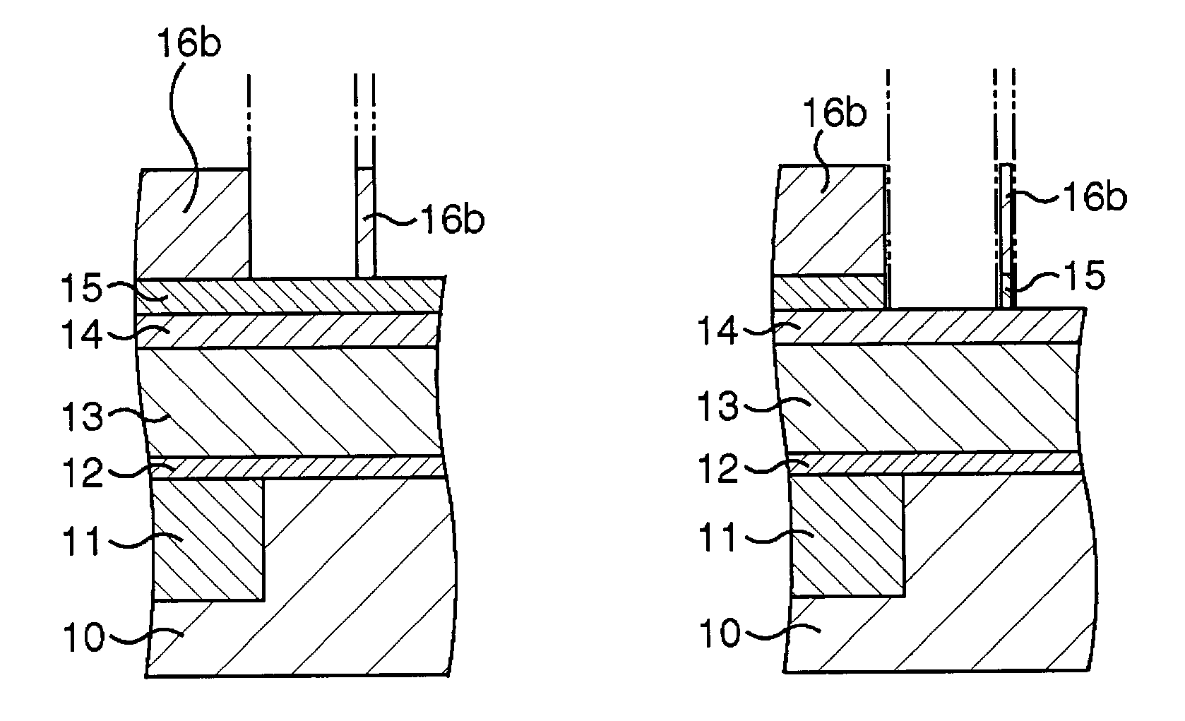
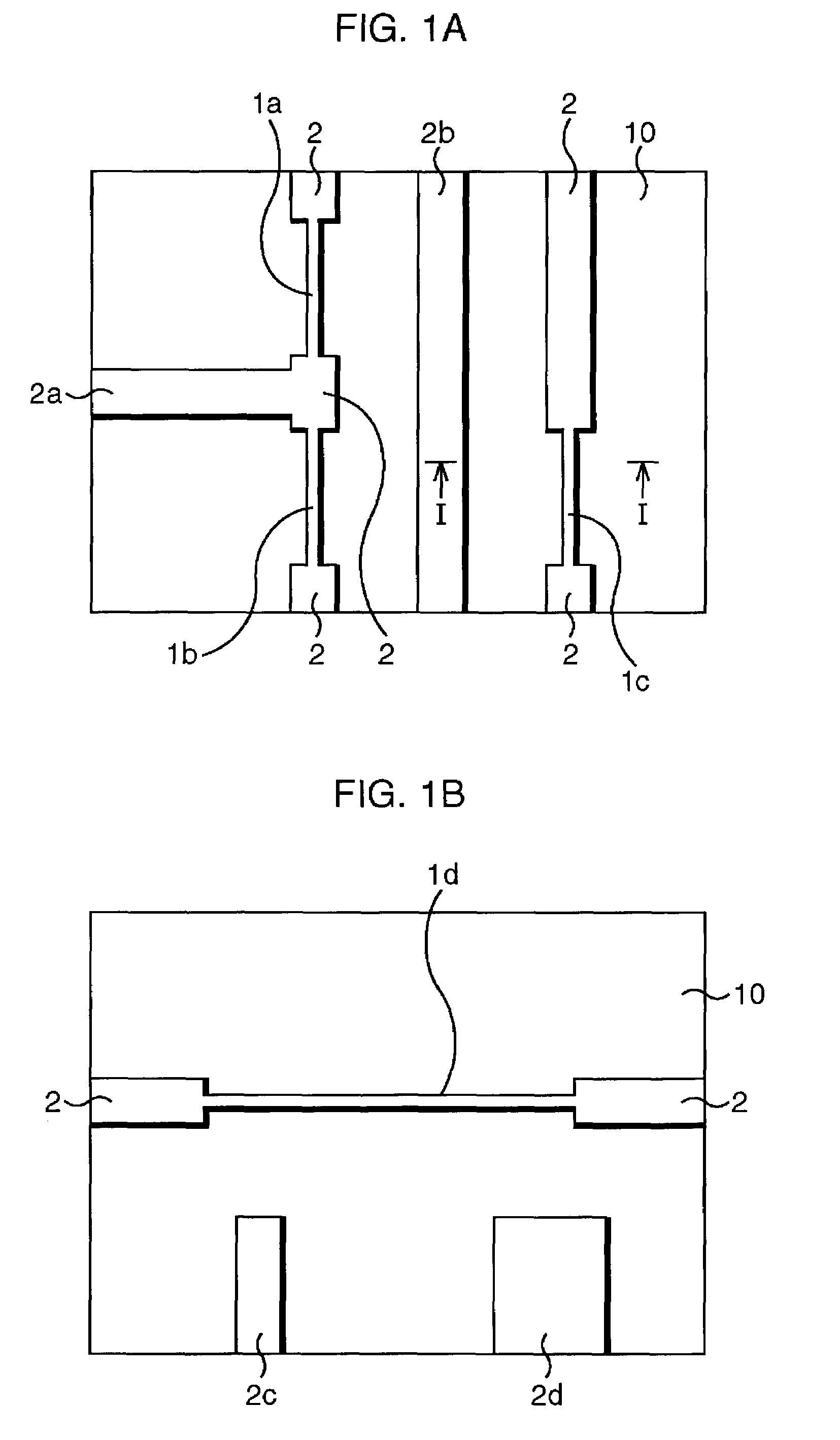
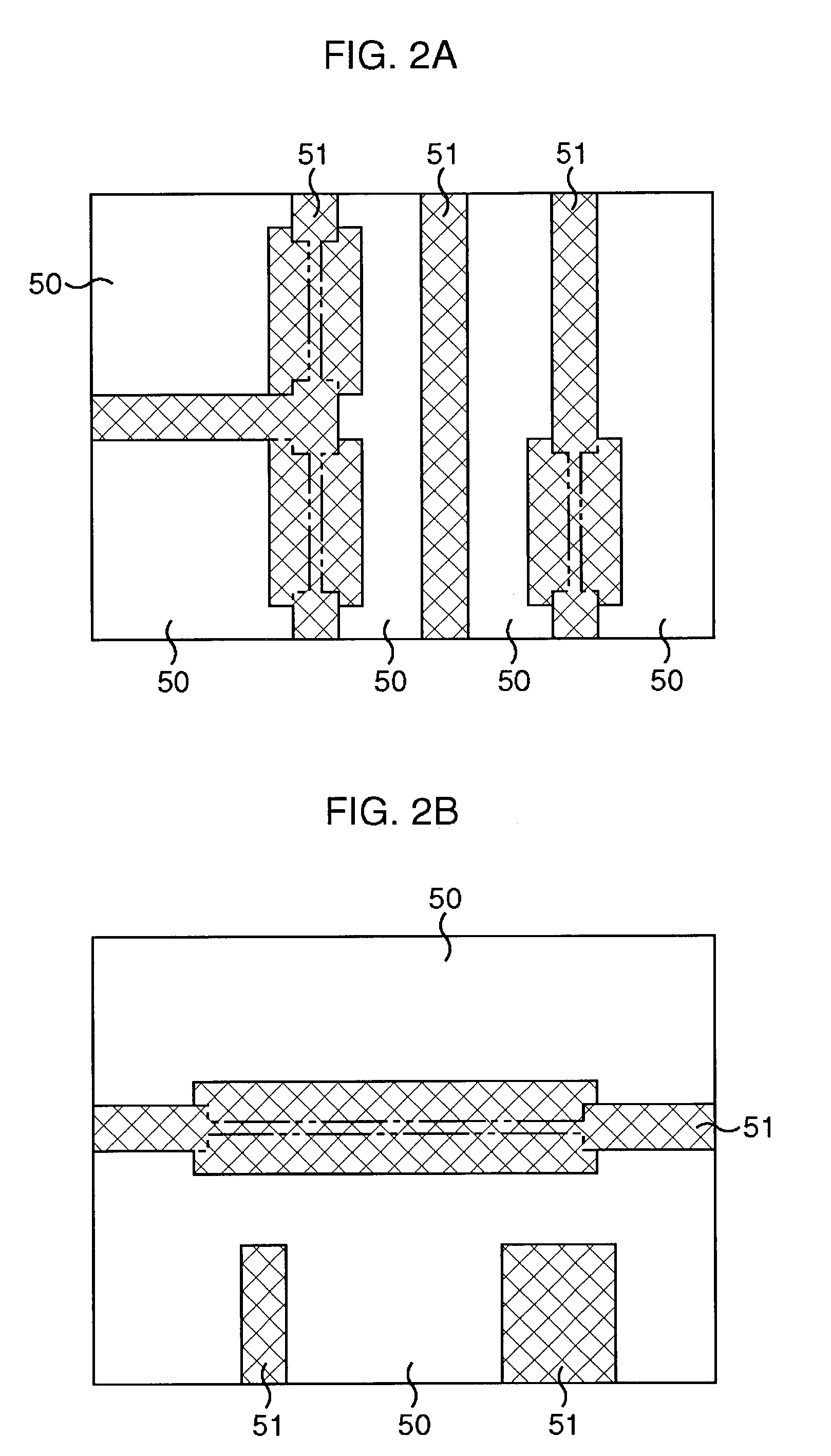
[0045]The first embodiment of the present invention will be explained first. FIG. 4A to FIG. 4K are sectional views showing a method of manufacturing a semiconductor device relating to the first embodiment of the present invention in process order. Incidentally, FIG. 4A to FIG. 4K correspond to a sectional view along the line I—I in FIG. 1A. FIGS. 5A and 5B to FIGS. 8A and 8B are plan views corresponding to states shown in FIG. 4B, FIG. 4D, FIG. 4F, and FIG. 4I respectively.

[0046]First, as shown in FIG. 4A, above a semiconductor substrate 10 on the surface of which an element isolating and insulating film 11 is formed, a gate oxidation film 12, a polycrystalline silicon film 13, a hard mask 14, an antireflection film 15, and a resist film 16 are formed in sequence. The thicknesses of the gate oxidation film 12, the polycrystalline silicon film 13, the hard mask 14, the antireflection film 15, and the resist film 16 are, for instance, 2 nm, 100 nm, 50 nm, 60 n...

second embodiment -

[0059]-Second Embodiment-

[0060]The second embodiment of the present invention will be explained next. FIG. 9A to FIG. 9K are sectional views showing a method of manufacturing a semiconductor device relating to the second embodiment of the present invention in process order. Incidentally, FIG. 9A to FIG. 9K correspond to sectional views along the line I—I in FIG. 1A. FIGS. 10A and 10B to FIGS. 13A and 13B are plan views corresponding to FIG. 9B, FIG. 9E, FIG. 9G, and FIG. 9I.

[0061]First, as shown in FIG. 9A, above a semiconductor substrate 10 on the surface of which an element isolating and insulating film 11 is formed, a gate oxidation film 12, a polycrystalline silicon film 13, a hard mask 14, an antireflection film 15, and a resist film 16 are formed in sequence, similarly to the first embodiment.

[0062]Then, the resist film 16 is exposed using gate electrode formation masks shown in FIG. 3A and FIG. 3B. Concretely, a Levenson phase shift mask and a reduction projection type aligne...


PUM

PropertyMeasurementUnit
transmittanceaaaaaaaaaa
thicknessesaaaaaaaaaa

Abstract

A resist pattern of a resist film is formed by exposing the resist film using a gate electrode forming mask (a Levenson phase shift mask), and developing the resist film. An antireflection film is etched using the resist pattern as an etching mask, and the resist pattern and the antireflection film are trimmed. The manner of this trimming is not to etch a hard mask made of an inorganic material, but to etch the resist pattern and the antireflection film made of an organic material. Since a region consistent with a wiring pattern of the hard mask is covered by the resist pattern completely, breaking down and retraction of the wiring are prevented.

Description

CROSS-REFERENCE TO RELATED APPLICATIONS[0001]This application is based upon and claims the benefit of priority from the prior Japanese Patent Application No. 2002-120991, filed on Apr. 23, 2002, the entire contents of which are incorporated herein by reference.BACKGROUND OF THE INVENTION[0002]1. Field of the Invention[0003]The present invention relates to a method of manufacturing a semiconductor device including a step of patterning one layer using a plurality of reticles.[0004]2. Description of the Related Art[0005]With recent miniaturization of semiconductor devices, formation of miniaturized wirings and miniaturized pitches are required. Consequently, a multiple exposure process using a plurality of reticles (exposure masks) is introduced for patterning of one layer.[0006]The multiple exposure process comprises the steps of, first, forming a layer to be patterned on or above a semiconductor substrate to form a resist film thereon by coating. Then, a first sheet of the reticle is...

Claims


Application Information

Patent Timeline
Patent Type & Authority Patents(United States)
IPC IPC(8): H01L21/28H01L21/027H01L21/3213H01L29/423H01L29/49H01L29/78
CPCH01L21/0273H01L21/32139H01L21/28035
Inventor MINAMI, TAKAYOSHI
Owner FUJITSU SEMICON LTD
Why Eureka
Try Eureka