Method of manufacturing a thinned gate electrode utilizing protective films and etching

Inactive Publication Date: 2005-02-01
RENESAS ELECTRONICS CORP
View PDF0 Cites 2 Cited by
  • Summary
  • Abstract
  • Description
  • Claims
  • Application Information

AI Technical Summary

Benefits of technology

[0012]An object of the invention is to provide a semiconductor device and a manufacturing method thereof in which the reduction of length of the gate electrode can be suppressed when it is thinned.
[0014]In the step (d), the second protective film used as a mask prevents the first protective film from being shortened in the length direction. As a result the gate electrode formed in the step (e) is not shortened, either, and therefore it is not necessary to size the first resist mask longer prior to the thinning process, which contributes to achievement of higher integration of the semiconductor device. On the other hand, the part of the gate electrode which lies on the active region is thinned and therefore the gate length (channel length) is shortened, which contributes to achievement of higher operation speed of the semiconductor device.
[0016]In the step (e), the second protective film used as a mask prevents the gate electrode from being shortened in the length direction. As a result it is not necessary to size the first protective film longer prior to the thinning process, which contributes to achievement of higher integration of the semiconductor device. On the other hand, the part of the gate electrode which lies on the active region is thinned and therefore the gate length (channel length) is shortened, which contributes to achievement of higher operation speed of the semiconductor device.

Problems solved by technology

However, since the resolution in lithography is limited by the limited wavelength of the light source, it is difficult to form gate electrodes having widths of about 100 nm or less by using common gate electrode formation process; therefore the methods shown below are used to form such thin gate electrodes.
However, forming a longer resist mask 105 increases the chip size and therefore hinders achievement of higher integration of the semiconductor device.
That is, this manufacturing method, too, raises the problem described referring to FIGS. 25A and 25B.
This requires that the gate electrode be designed longer in advance, considering the reduction of length (i.e. in the processes shown above, forming a longer resist mask 105 (or 107) before it is thinned), or that larger pads be designed at both ends of the gate electrode to which interconnections are connected, but such approaches result in an increase in chip size.

Method used


Image

  • Method of manufacturing a thinned gate electrode utilizing protective films and etching
  • Method of manufacturing a thinned gate electrode utilizing protective films and etching
  • Method of manufacturing a thinned gate electrode utilizing protective films and etching

Examples


Embodiment Construction

to a sixth preferred embodiment;

[0026]FIGS. 21A and 21B are diagrams used to describe a method for forming a pattern for the second protective film according to a seventh preferred embodiment;

[0027]FIGS. 22A and 22B to 24A and 24B are process diagrams showing a conventional semiconductor device manufacturing method;

[0028]FIGS. 25A and 25B are diagrams used to describe a problem of the conventional semiconductor device; and

[0029]FIGS. 26A and 26B to 29A and 29B are process diagrams showing a conventional semiconductor device manufacturing method.

DESCRIPTION OF THE PREFERRED EMBODIMENTS

[0030]

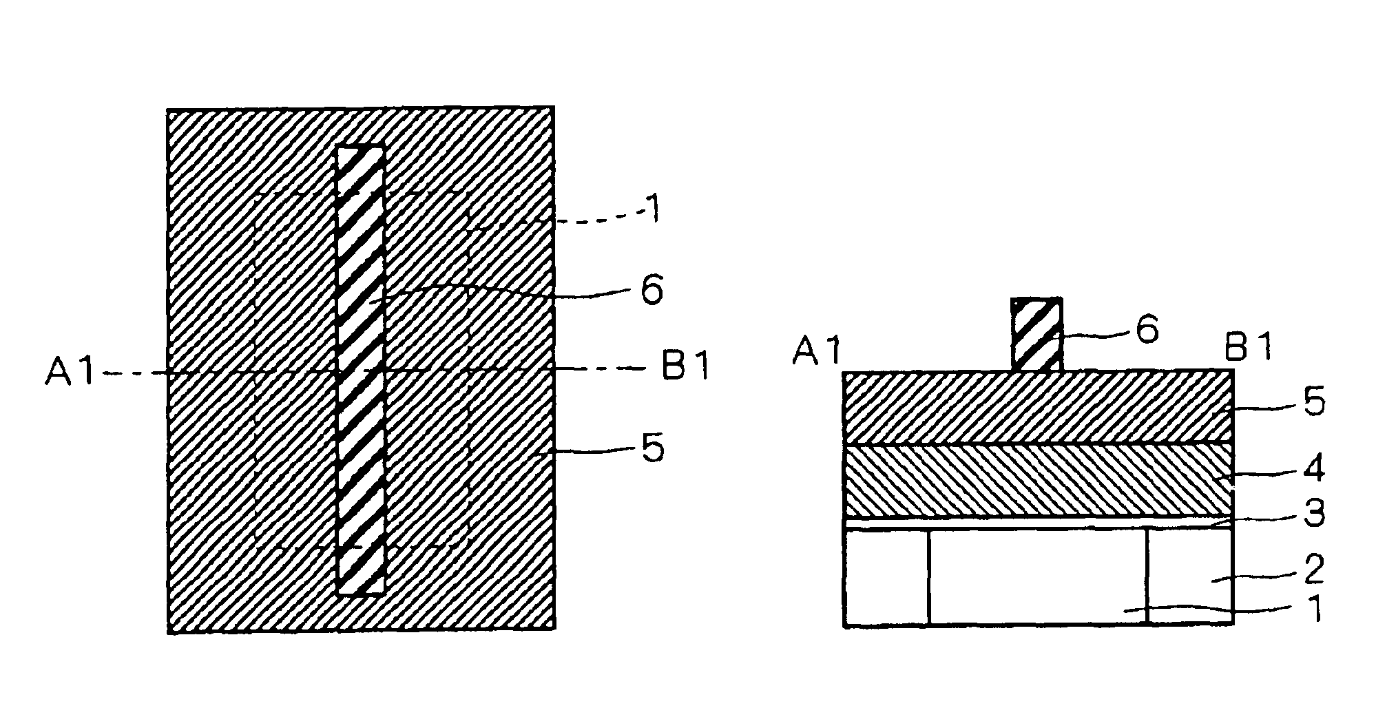
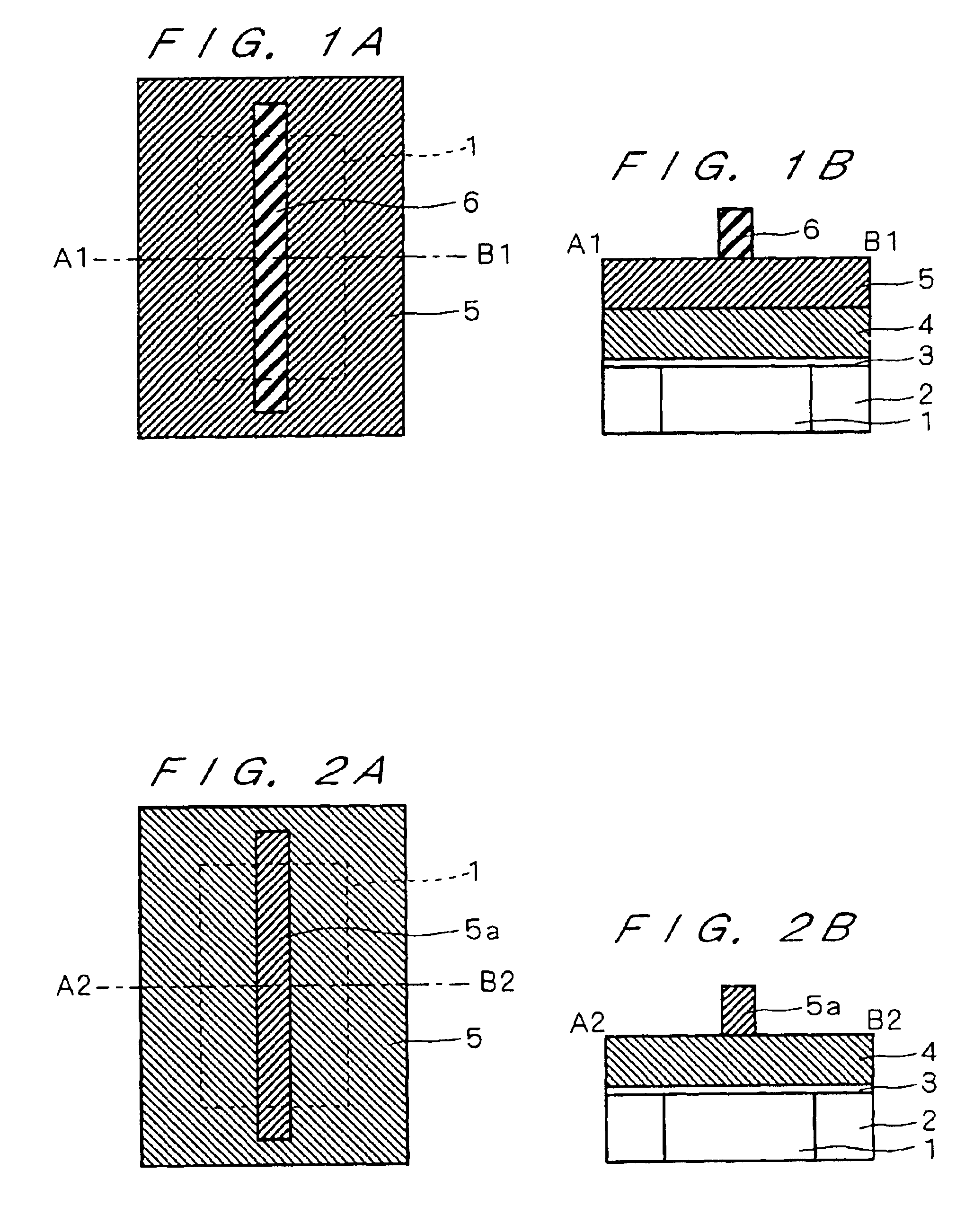
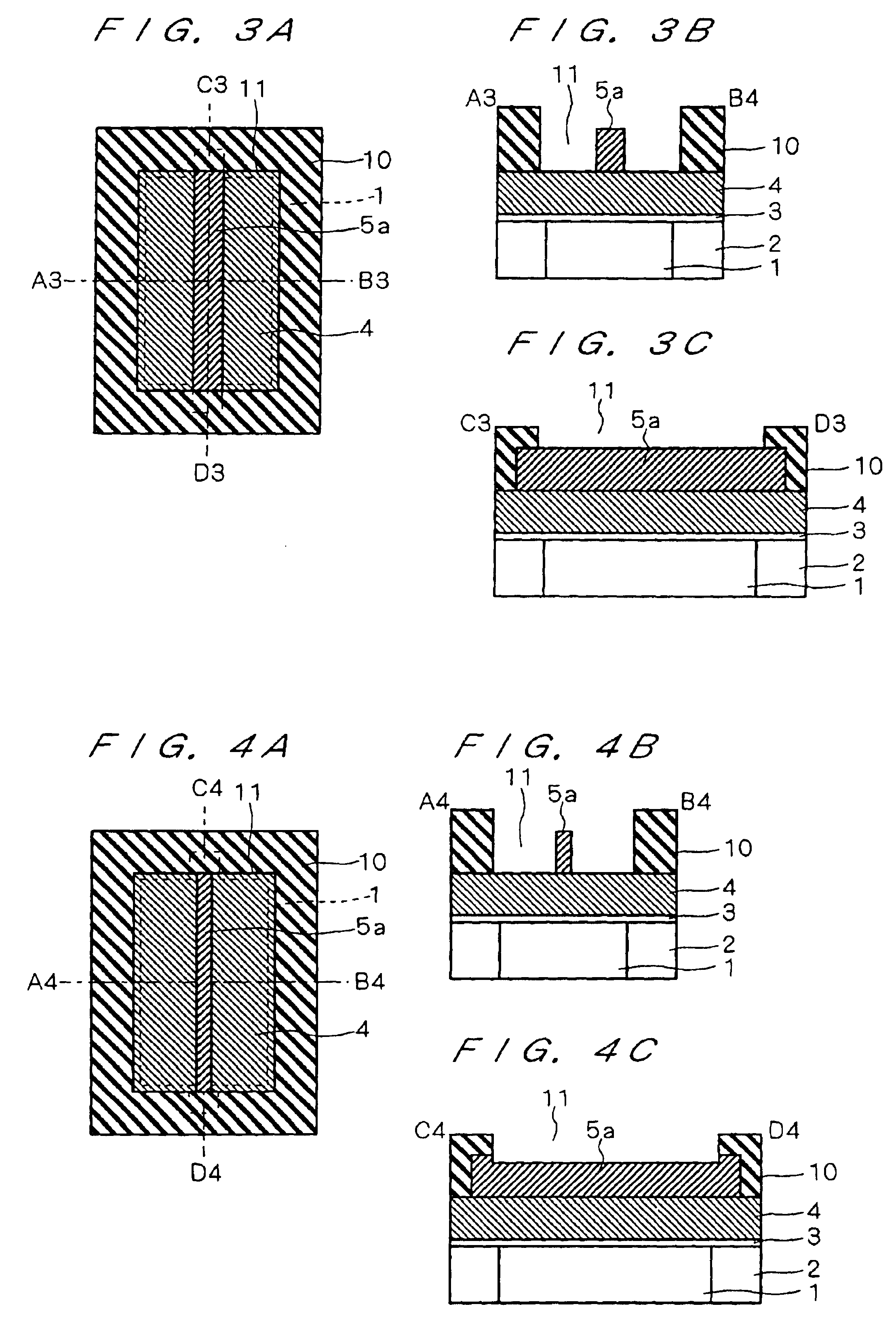
[0031]FIGS. 1A, 1B, 2A, 2B, 3A, 3B, 3C, 4A, 4B, 4C, 5A, 5B, 6A, 6B and 6C are process diagrams showing a semiconductor device manufacturing method according to a first preferred embodiment. In these diagrams, FIG. 1B shows the cross section taken along the direction A1-B1 in FIG. 1A, FIG. 2B shows the cross section taken along the direction A2-B2 in FIG. 2A, FIGS. 3B and 3C show the cross sections...


PUM


Abstract

The reduction of length of a gate electrode is suppressed in the process of thinning it. A hard mask (5a) is thinned and used to etch a gate electrode material film (4) to form a gate electrode. At this time, a resist mask (10) having an opening (11) over an active region (1) is formed; the resist mask (10) covers at least both ends in the length direction of the hard mask (5a) and exposes in the opening (11) at least the entirety of the part of the hard mask (5a) which lies right above the active region (1). The hard mask (5a) is thinned by etching using the resist mask (10) as a mask and therefore the hard mask (5a) is thinned in the part over the active region (1) without being shortened in the length direction. As a result, the gate electrode formed by using the thinned hard mask (5a) is not shortened in length.

Description

BACKGROUND OF THE INVENTION[0002]1. Field of the Invention[0003]The present invention relates to a semiconductor device having a gate electrode and its manufacturing method, and particularly to a technique for thinning the gate electrode.[0004]2. Description of the Background Art[0005]The requirements of making finer circuit patterns for more highly integrated semiconductor devices are constantly bringing about finer gate electrode structures. Also, the technique for reducing the gate length (channel length) of transistors, i.e. for thinning the gate electrode structures, is important for the purpose of increasing the speed of devices. However, since the resolution in lithography is limited by the limited wavelength of the light source, it is difficult to form gate electrodes having widths of about 100 nm or less by using common gate electrode formation process; therefore the methods shown below are used to form such thin gate electrodes.[0006]FIGS. 22A, 22B, 23A, 23B, 24A and 24B a...

Claims


Application Information

Patent Timeline
IPC IPC(8): H01L21/02H01L21/033H01L21/027H01L21/28H01L21/3213H01L21/3065H01L29/423H01L29/49H01L29/78
CPCH01L21/0273H01L21/0334H01L21/32139H01L21/28123H01L21/0337H01L21/18
Inventor YAMADA, TETSUYAUENO, ATSUSHITSUJITA, KOUICHIROUYAMAGUCHI, ATSUMIOKAGAWA, TAKASHI
Owner RENESAS ELECTRONICS CORP
Why Eureka
Try Eureka