
Composite material

a technology of composite materials and materials, applied in the field of composite materials, can solve the problems of increasing the temperature of those semiconductor devices, the ineffectiveness of the semiconductor device to sufficiently radiate heat generated, and the large amount of electric power consumed by power transistors and semiconductor rectifiers per operating area, so as to prevent interfacial reaction, promote oxide film generation, and avoid the coefficient of thermal conductivity of the porous ceramic sintered body

Inactive Publication Date: 2005-10-11
NGK INSULATORS LTD
View PDF10 Cites 3 Cited by
  • Summary
  • Abstract
  • Description
  • Claims
  • Application Information

AI Technical Summary

Benefits of technology

[0017]Another object of the present invention is to provide a composite material which can increase an impregnation ratio of a metal to a porous ceramic sintered body resulting in the metal being easily impregnated into the porous ceramic sintered body, which can increase the productivity of a heat sink having characteristics balanced against the coefficient of thermal expansion and the coefficient of thermal conductivity of actual electronic parts (including semiconductor devices).
[0041]The thickness of the oxide film varies depending on the impregnating conditions under which the oxide film is impregnated with the copper alloy. The impregnating conditions determine the thickness of the oxide film which is optimum for the suppression of the interfacial reaction. The thickness of the oxide film should preferably be in the range from 0.01 μm to 10 μm. If the thickness of the oxide film is too large, then the oxide film acts as a thermal barrier between the porous ceramic sintered body and the copper alloy, tending to lower the coefficient of thermal conductivity of the composite material according to the present invention.

Problems solved by technology

Semiconductor devices such as power transistors and semiconductor rectifiers consume a large amount of electric power per operating area, and cases (packages) and leads of such semiconductor devices may not be effective enough to sufficiently radiate heat generated thereby.
Therefore, the internal temperature of those semiconductor devices tend to increase to such a level that the semiconductor devices may suffer a thermal breakdown.
Semiconductor devices of greater size are liable to peel off position or be mechanically broken due to increased stresses which are caused by the difference between the coefficient of thermal expansion of the semiconductor substrate (silicon substrate or GaAs substrate) and the coefficient of thermal expansion of the heat sink.
Therefore, the theoretical values cannot be balanced against the coefficient of thermal expansion and the coefficient of thermal conductivity of actual electronic parts.
The heat sink material according to the conventional example 2 suffers a limitation on efforts to increase the coefficient of thermal conductivity as the ratio of Cu impregnated in the powder-sintered porous body is low.

Method used


Image

  • Composite material
  • Composite material
  • Composite material

Examples


first embodiment

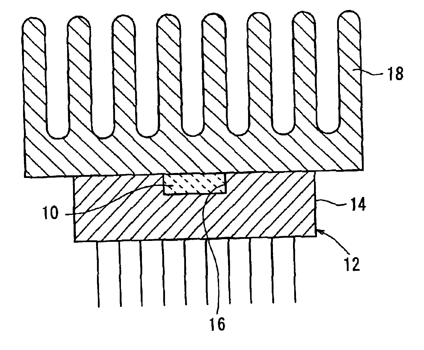
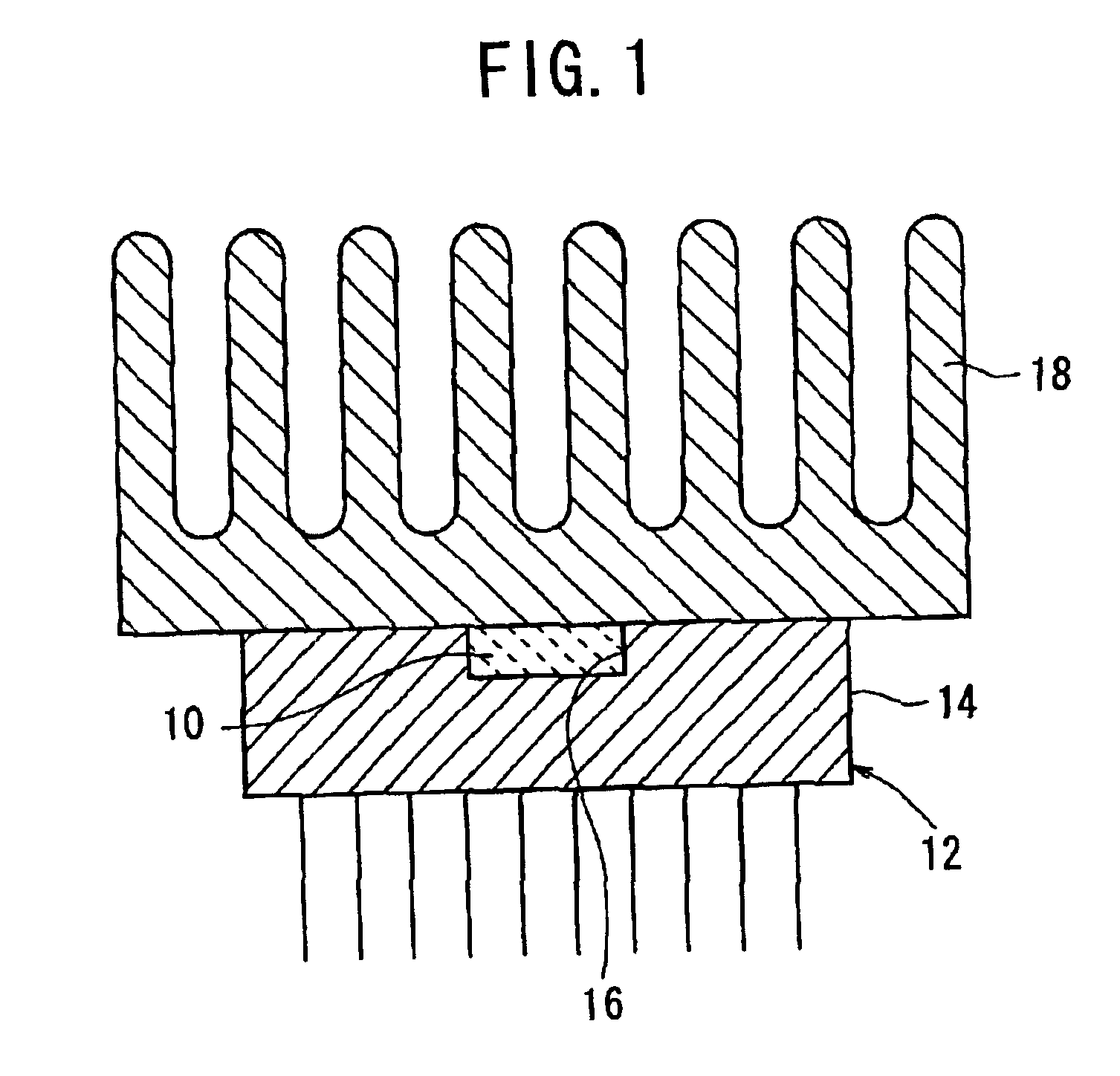
[0077]As shown in FIG. 1, a heat sink 10 made of a composite material according to the present invention is embedded in an opening 16 defined in an upper surface of a package 14 of a semiconductor device 12 and has a surface held in contact with cooling fins 18 fixed to the upper surface of the package 14.

[0078]Heat radiated from a semiconductor element (chip) mounted in the semiconductor device 12 is efficiently transferred through the heat sink 10 to the cooling fins 18.

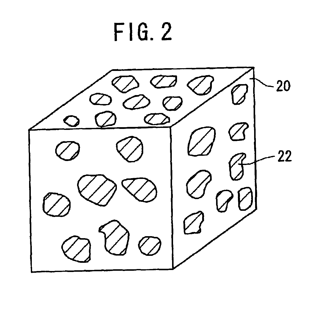
[0079]The composite material according to the first embodiment of the present invention comprises a porous ceramic sintered body produced by preliminarily sintering a porous body having a coefficient of thermal expansion lower than the coefficient of thermal expansion of copper to construct a network therein, the porous ceramic sintered body being impregnated with a copper alloy. Specifically, as shown in FIG. 2, a porous ceramic sintered body 20 of SiC has open pores impregnated with a copper alloy 22. The porous ...

second embodiment

[0141]A method of manufacturing a composite material according to the present invention will be described below with reference to FIGS. 10 to 15.

[0142]The method of manufacturing the composite material according to the second embodiment employs a hot press furnace 60 shown in FIG. 10. The hot press furnace 60 comprises a tubular housing 62 accommodating therein a lower punch 64 serving as a base, an upwardly open refractory casing 66 fixedly mounted on the lower punch 64, an upper punch 68 movable into and out of the refractory casing 66 through its upper opening, and a heater 70 for heating the refractory casing 66. The hot press furnace 60 has a suction pipe 72 for evacuating the housing 62.

[0143]The refractory casing 66 is of a tubular shape with a space 74 defined therein. The upper punch 68 has a flange 76 on its side wall for determining the stroke thereof. A packing 78 is attached to the lower surface of the flange 76 for contacting the upper end surface of the refractory cas...

third embodiment

[0167]A method of manufacturing a composite material according to the present invention will be described below with reference to FIGS. 16 and 17. Those parts in FIG. 16 which are identical to those shown in FIG. 10 are denoted by identical reference characters, and will not be described in detail below.

[0168]The method of manufacturing the composite material according to the third embodiment is essentially the same in principle as the method of manufacturing the composite material according to the second embodiment, but differs therefrom in that in the impregnating process, the SiC 20 and the copper alloy 22 are brought into contact with each other under a negative pressure or normal pressure, and then heated to melt the copper alloy 22.

[0169]Specifically, as shown in FIG. 16, the filter 54 is not charged, but bodies of the SiC 20 and masses of the copper alloy 22, which are arranged successively upwardly in the order named, are charged into the refractory casing 66 of the hot pres...


PUM

PropertyMeasurementUnit
Temperatureaaaaaaaaaa
Fractionaaaaaaaaaa

Abstract

A composite material includes an SiC porous ceramic sintered body, which is formed by preliminarily sintering a porous body, having a coefficient of thermal expansion lower than the coefficient of thermal expansion of copper to construct a network therein. A copper alloy impregnating the porous ceramic sintered body includes copper and one or more additive elements which are prepared to impart a coefficient of thermal conductivity of 160 W / mK or higher to the composite material. The additive elements include up to 5% of at least one element selected from Be, Al, Si, Mg, Ti, Ni, Bi, Te, Zn, Pb, Sn, and mish metal, and also contain unavoidable impurities and gas components.

Description

BACKGROUND OF THE INVENTION[0001]1. Field of the Invention[0002]The present invention relates to a composite material having an inorganic material or an oxide film thereof which is impregnated with a metal, and more particularly to a composite material for use in a heat sink such as a semiconductor heat sink for efficiently radiating heat generated by a semiconductor device, for example.[0003]2. Description of the Related Art[0004]Generally, semiconductor devices are highly susceptible to heat, and should be designed such that their internal temperature will not exceed an allowable maximum temperature at a junction area of said semiconductor devices. Semiconductor devices such as power transistors and semiconductor rectifiers consume a large amount of electric power per operating area, and cases (packages) and leads of such semiconductor devices may not be effective enough to sufficiently radiate heat generated thereby. Therefore, the internal temperature of those semiconductor devi...

Claims


Application Information

Patent Timeline
IPC IPC(8): B32B15/04C04B41/88C22C9/00H01L23/34H01L23/373H01L23/12H01L23/15C04B41/51C04B41/52C04B41/90C22C1/10C22C9/01C22C9/05C22C9/06C22C9/10H01L21/48
CPCC04B41/009C04B41/52C04B41/88C04B41/90C22C1/1036C22C9/00C22C9/01C22C9/05C22C9/06C22C9/10H01L21/4871H01L23/3733C04B41/5127C04B41/4521C04B41/4523C04B41/0072C04B41/4556C04B41/5027C04B41/5035C04B41/522C04B41/457C04B35/08C04B35/565C04B35/584C04B35/581C04B35/563C04B38/00Y10T428/12611C04B2111/00844Y10T428/12576H01L2924/0002H01L2924/00Y10T428/249957Y10T428/24997Y10T428/249974
Inventor ISHIKAWA, SHUHEIMITSUI, TSUTOMUSUZUKI, KENNAKAYAMA, NOBUAKITAKEUCHI, HIROYUKIYASUI, SEIJI
Owner NGK INSULATORS LTD
Learn More