Method for fabricating a packaging substrate

a packaging substrate and manufacturing method technology, applied in the field of circuit boards, can solve the problems of sacrificing the surface area of functional circuit layout patterns, adversely affecting chip performance, and introducing substantial yield and cost challenges, so as to achieve effective prevention of scratches or collision damage, the effect of reducing the cost per substrate and avoiding metal peeling

Active Publication Date: 2005-08-16
NAN YA PRINTED CIRCUIT BOARD CORPORATION
View PDF5 Cites 12 Cited by
  • Summary
  • Abstract
  • Description
  • Claims
  • Application Information

AI Technical Summary

Benefits of technology

[0015]The present invention comprises at least the following advantages. First, the cost per substrate is reduced since there is no need to coat an additional conductive metal layer for electroplating after the definition of circuit pattern layout. The conductive materials used to assist electroplating include the thin copper base layer and the chemically deposited copper layer. The potential scratch or collision damages can be effectively prevented since the entire circuit pattern is revealed at a later fabrication stage.
[0016]Further, metal peeling is avoided thereby promoting the production yield. Moreover, sidewalls of the circuit pattern in the Au-plating area are also covered by Ni / Au film and thus avoiding overhang problem.

Problems solved by technology

While high-density packages such as flip-chip and BGA devices permit very high input-output (I / O) counts, the resulting close dimensions introduce substantial yield and cost challenges.
However, These conducting wires occupy a large amount of area, thus leading to sacrificing the surface area for functional circuit layout pattern.
Another drawback of employing plating bus is that when operating at high frequency, noise due to the antenna effect may occur, and thus adversely affecting chip performance.
First, the process is costly because an additional metallization is needed after the patterning of circuit lines on the substrate.
In addition, the fine conductive lines on the substrate might be unwarily scratched or damaged due to collision.
Furthermore, metal peeling problem is also an issue that potentially affecting the production yield.
However, the process disclosed in this patent has a Ni / Au overhang problem due to that the sidewalls of the contact pad are not covered by the Ni / Au layer.
The exposed sidewalls of the contact pads may be oxidized resulting in short circuiting or reliability concerns.

Method used


Image

  • Method for fabricating a packaging substrate
  • Method for fabricating a packaging substrate
  • Method for fabricating a packaging substrate

Examples


Embodiment Construction

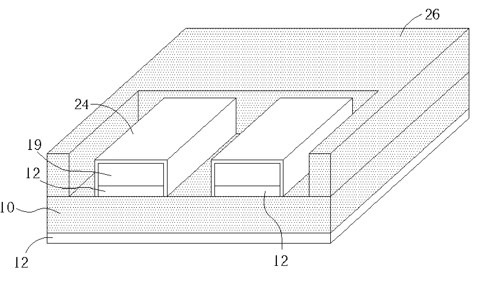
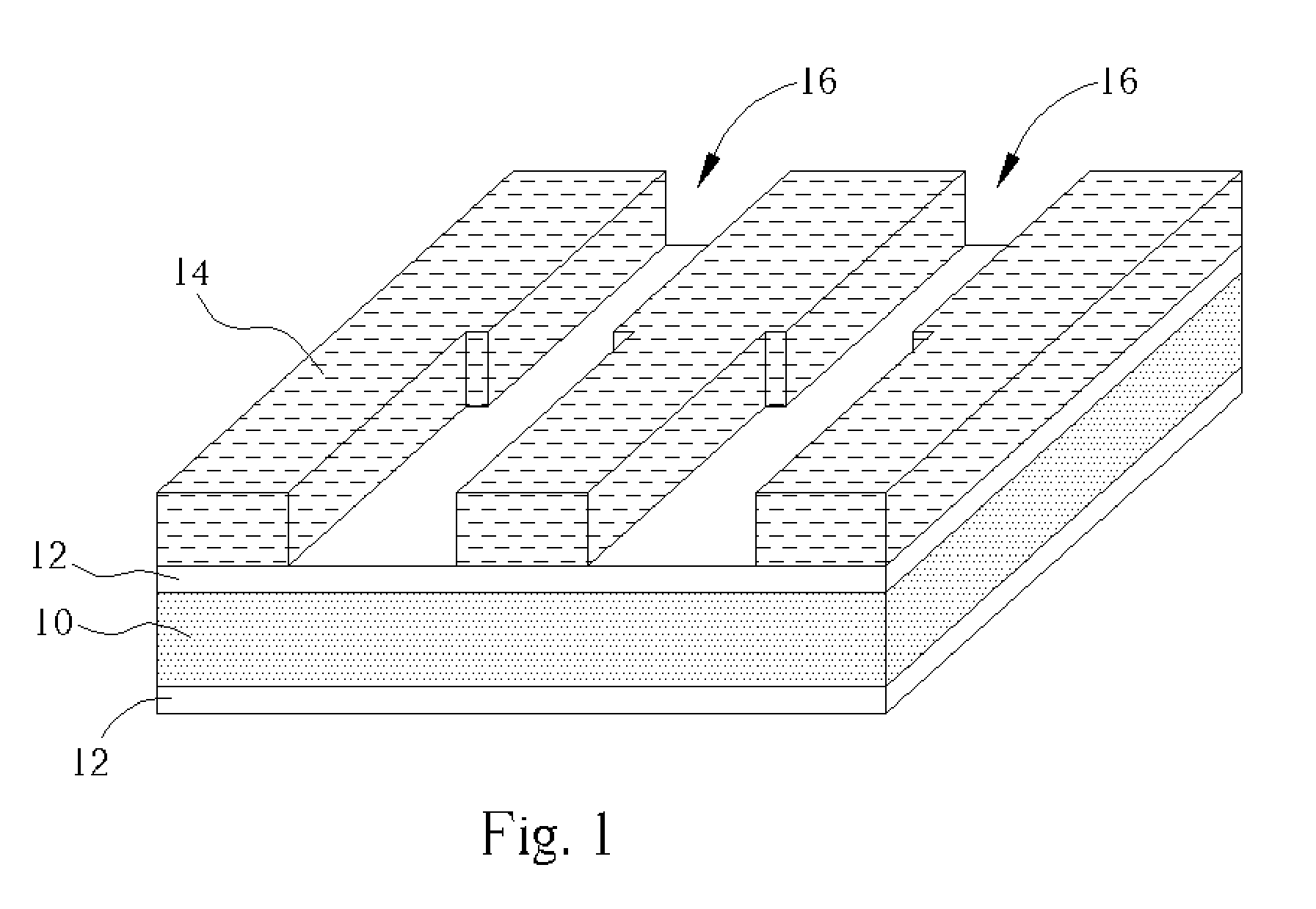
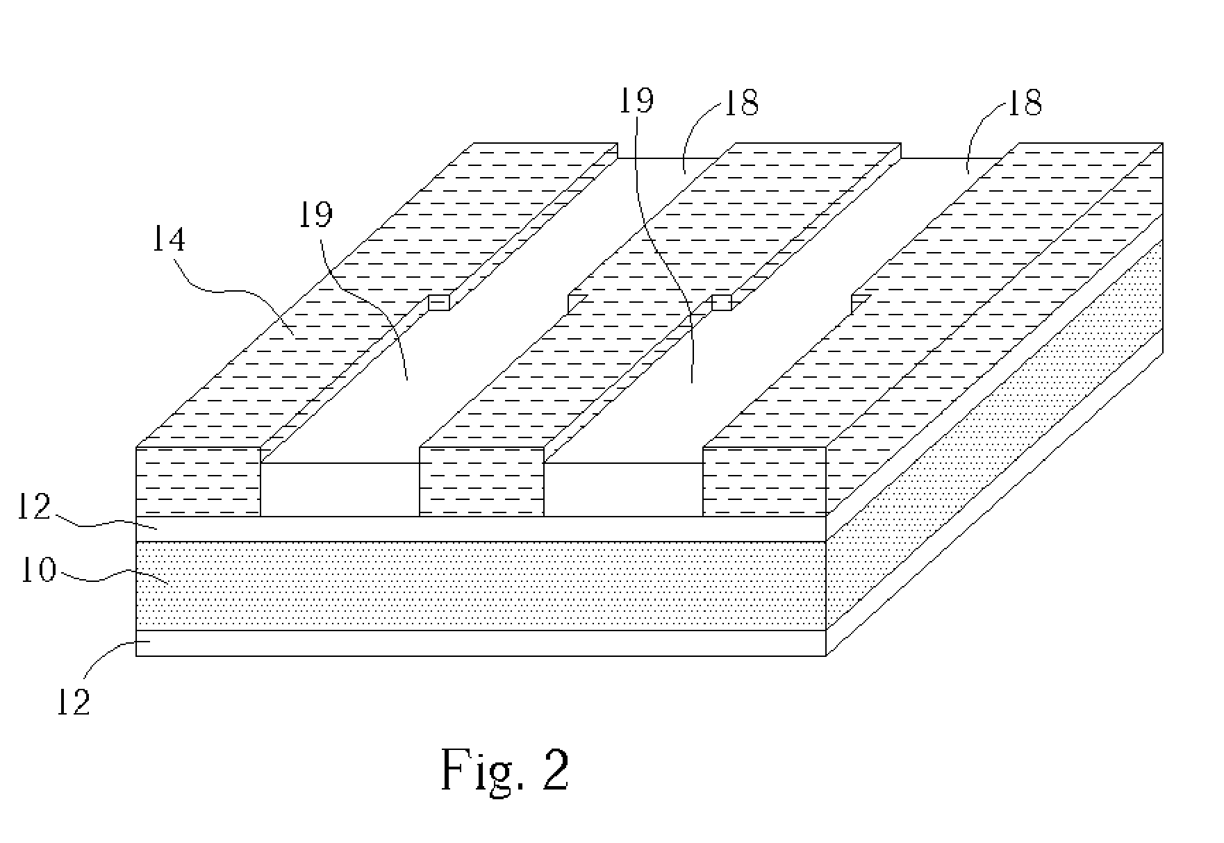
[0020]One preferred embodiment of the method of manufacturing packaging substrate in accordance with the present invention will be explained as follows referring to FIG. 1 to FIG. 10. FIG. 1 to FIG. 10 are perspective cross-sectional diagrams illustrating the present invention method of making a packaging substrate, which utilizes two selective etching steps to define Au-plating area and non-Au-plating area, and utilizes three photo image transferring steps.

[0021]As shown in FIG. 1, a carrier plate 10 made of insulating materials such as plastic is prepared. A number of via through holes or blind via hole (not shown) have been drilled in the carrier plate 10 by using conventional mechanical drilling or Laser drilling methods or the like. It is understood that the via through holes or blind via hole are not shown because they are known in the art and they are substantially not germane to the present invention. Via metallization process is then carried out to form a thin copper base l...


PUM

PropertyMeasurementUnit
thicknessaaaaaaaaaa
thicknessaaaaaaaaaa
areaaaaaaaaaaa

Abstract

A method for making a packaging substrate is provided. A thin copper seed layer is formed on a carrier plate. A first resist layer is coated on the thin copper seed layer. The first resist layer defines a wire layout of copper plating area. A layer of copper is then electroplated on the copper plating area to form the wire layout. After this, the first resist layer is stripped to expose the wire layout and the thin copper seed layer. A patterned second resist layer is formed on the wire layout. The patterned second resist layer defines the Ni / Au plating area of the wire layout. The copper seed layer that is not covered by the second resist layer is etched away. A third resist layer is stacked on the second resist layer and defines an Au-plating area of the I / O fingers. Using the third resist layer as a plating hard mask, a layer of Ni / Au layer is plated on the exposed area of the wires. After this step, the second and third resist layers are removed.

Description

BACKGROUND OF INVENTION[0001]1. Field of the Invention[0002]The present invention relates generally to the field of circuit boards. More particularly, the present invention relates to a method for manufacturing a packaging substrate. Two selective etching steps are utilized to define the Au-plating area and the non-Au-plating area.[0003]2. Description of the Prior Art[0004]As the functionality and performance of network systems, high-end servers, and mobile communication devices improves, the demand for high-performance, high pin count packages is increasing. This increasing demand requires new technologies, which incorporate high pin count and also delivers performance via impedance control, low crosstalk, DC / AC resistance, and low VG impedance. Sophisticated interconnect technology has become essential for meeting these needs by improving the density and reliability of the substrates for LSI package and module boards. While high-density packages such as flip-chip and BGA devices p...

Claims


Application Information

Patent Timeline
Patent Type & Authority Patents(United States)
IPC IPC(8): H01L21/02H01L21/44H01L21/48H05K3/06H05K3/10H05K3/24
CPCH01L21/4846H05K3/243H05K3/064H05K3/108H05K2203/1476H05K2203/0571H05K2203/0577H05K2203/0597
Inventor WENG, YI-TANG
Owner NAN YA PRINTED CIRCUIT BOARD CORPORATION
Why Eureka
Try Eureka