
Thin film ink jet printhead adhesion enhancement

a technology of thin film ink jet and printhead, which is applied in printing and other directions, can solve the problems of heater failure, significant delamination between ta layer and dielectric layer, mechanical shock to the thin metal layer comprising the ink ejection device, etc., and achieves significant increase in adhesion, little or no added cost, and enhanced adhesion

Inactive Publication Date: 2005-08-16
FUNAI ELECTRIC CO LTD
View PDF13 Cites 9 Cited by
  • Summary
  • Abstract
  • Description
  • Claims
  • Application Information

AI Technical Summary

Benefits of technology

The invention provides an ink jet printhead with improved adhesion between thin film layers. This is achieved by depositing layers of tantalum, titanium, or platinum on a semiconductor substrate and using an adhesion layer made of tantalum nitride, tantalum oxide, silicon nitride, or titanium nitride to enhance the adhesion between the layers. This improves the performance and functionality of the printhead, while also reducing material costs and energy consumption.

Problems solved by technology

After the ink is ejected, the bubble collapses causing mechanical shock to the thin metal layers comprising the ink ejection device.
However, due to higher processing temperatures such as for printhead chips produced containing CMOS devices, delamination between the Ta layer and the dielectric layer becomes a significant problem.
If the cavitation layer delaminates from the dielectric layer, ink will penetrate into cracks and corrode the dielectric layer and underlying heater layer which will result in heater failure.
In addition, heat transfer from the heater film to the ink will be degraded, thereby adversely affecting print quality.

Method used


Image

  • Thin film ink jet printhead adhesion enhancement
  • Thin film ink jet printhead adhesion enhancement
  • Thin film ink jet printhead adhesion enhancement

Examples


example

[0040]A 6 inch diameter silicon wafer was placed in a chemical vapor deposition chamber. In order to form a layer of Si-doped DLC on the silicon wafer, tetramethysilane gas was flowed into the chamber at 100 standard cubic centimeters per minute (sccm). Methane gas was also flowed into the chamber at 100 sccm. The chamber pressure was maintained at about 50 millTorrs. The RF power during the deposition process was 600 watts at an RF frequency of 13.6 Khz and the substrate bias voltage was 300 to 700 volts. The substrate was maintained at room temperature and the deposition rate for the process was 4200 Angstroms per minute. The Si-doped DLC layer was formed in about 30 seconds. The resulting Si-doped DLC had a film refractive index of 2.4 to 2.5 and a film stress of −5 to −7×10⁹ dynes / cm2.

[0041]Upon completion of the formation of the Si-doped DLC layer, the methane gas flow was discontinued and the tetramethylsilane flow rate was decreased to 50 sccm. Nitrogen gas at a flow rate of ...


PUM


Abstract

An ink jet printhead for an ink jet printer and method for making an improved printhead. The printhead includes a nozzle plate attached to a heater chip. The heater chip is a semiconductor substrate having a resistive layer deposited on the substrate, a dielectric layer deposited on the resistive layer, a cavitation layer for contact with ink, and an adhesion layer between the dielectric layer and cavitation layer. The adhesion layer is selected from the group consisting of tantalum nitride (TaN), tantalum oxide (TaO), silicon nitride (SiN), and titanium nitride (TiN), provided the adhesion layer and cavitation layer are selected so that the adhesion layer has no elemental component in common with the cavitation layer when the dielectric layer is comprised of SiC / SiN. Adhesion between the dielectric layer and cavitation layer is significantly enhanced by the invention.

Description

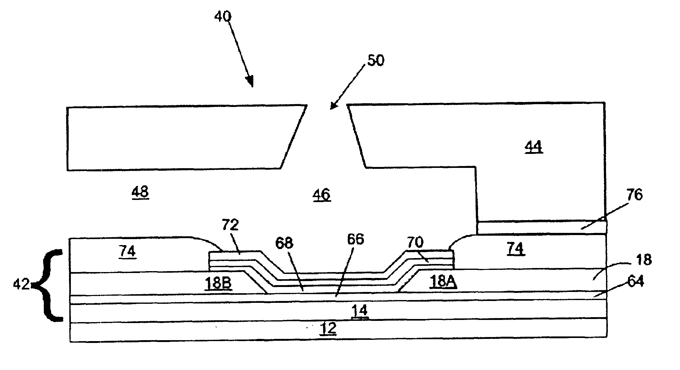
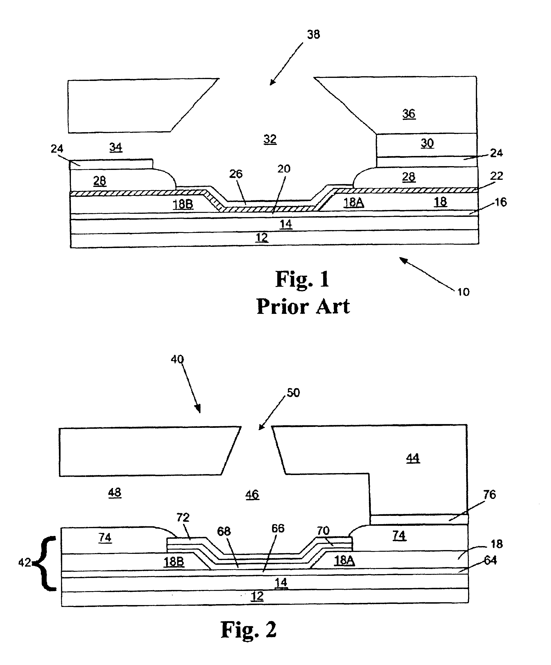
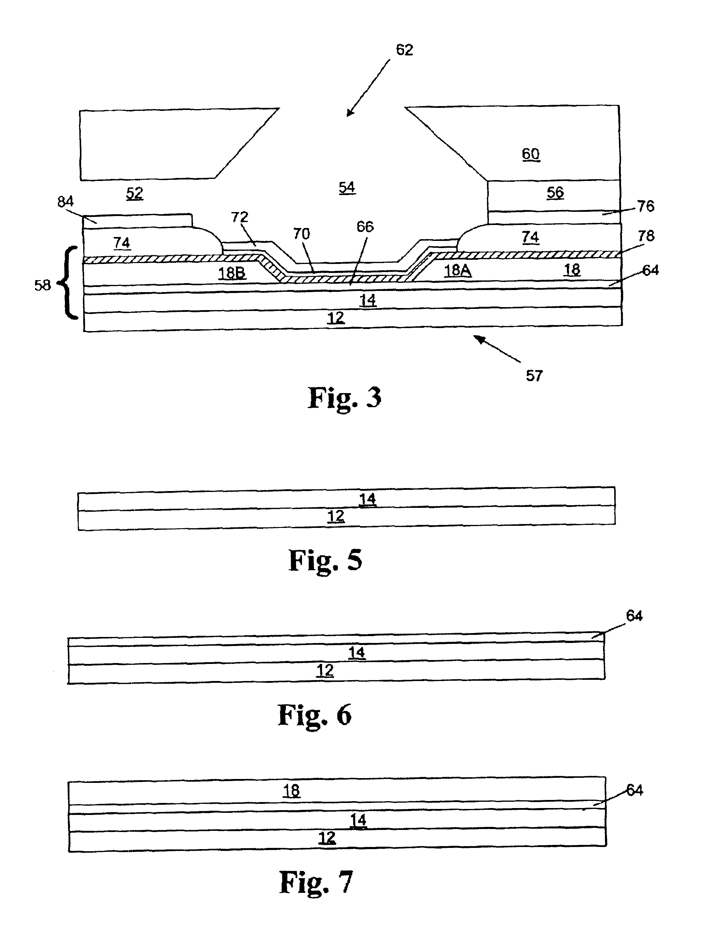
FIELD OF THE INVENTION[0001]The invention relates to compositions and methods that enhance adhesion between cavitation layer and an underlying dielectric layer for an ink jet printhead.BACKGROUND OF THE INVENTION[0002]In the production of ink jet printheads, a cavitation layer is typically provided as an ink contact layer. The cavitation layer is needed to prevent damage to the underlying dielectric and resistive layers during ink ejection. As ink is heated in an ink chamber by a heater resistor, a bubble is formed that forces ink out of the ink chamber and through an ink ejection orifice. After the ink is ejected, the bubble collapses causing mechanical shock to the thin metal layers comprising the ink ejection device. In a typical printhead, tantalum (Ta) is used as a cavitation layer. The Ta layer is deposited on a dielectric layer such as silicon carbide (SiC) or a composite layer of SiC and silicon nitride (SiN). In the composite layer, SiC is adjacent to the Ta layer.[0003]Und...

Claims


Application Information

Patent Timeline
Patent Type & Authority Patents(United States)
IPC IPC(8): B41J2/14
CPCB41J2/14129
Inventor BELL, BYRON V.GUAN, YIMIN
Owner FUNAI ELECTRIC CO LTD
Learn More