Silicon dual inertial sensors

a dual-inertial sensor and silicon technology, applied in the direction of acceleration measurement using interia force, turn-sensitive devices, instruments, etc., can solve the problems of large air damping, difficult to control the width the manufacturing process of the driving beam, etc., to achieve accurate control and reduce air damping

Inactive Publication Date: 2005-08-16
MIN OF NAT DEFENSE
View PDF2 Cites 25 Cited by
  • Summary
  • Abstract
  • Description
  • Claims
  • Application Information

AI Technical Summary

Benefits of technology

[0005]The major features of the present invention are: (1) dual inertial sensors made by etching (110) silicon chip whose width can be accurately controlled during the etching process; (2) the design to reduce the air damping of the (110) silicon proof-mass; (3) preventing the proof-mass from sticking to glass sheets; and (4) built-in temperature sensing capacitors placed in the chip area unaffected by the inertial force, and compensating the temperature error in the dual inertial sensors by direct measurement of the temperature changes in the chip.

Problems solved by technology

The major drawback of the aforementioned sensors is in the manufacturing process of the driving beams.
However, as there is no automatic mechanism to stop the etching as in the (111) facet, it is hard to control the width of the driving beam.
This poses a major problem for the quality of the products.

Method used


Image

  • Silicon dual inertial sensors
  • Silicon dual inertial sensors
  • Silicon dual inertial sensors

Examples


Embodiment Construction

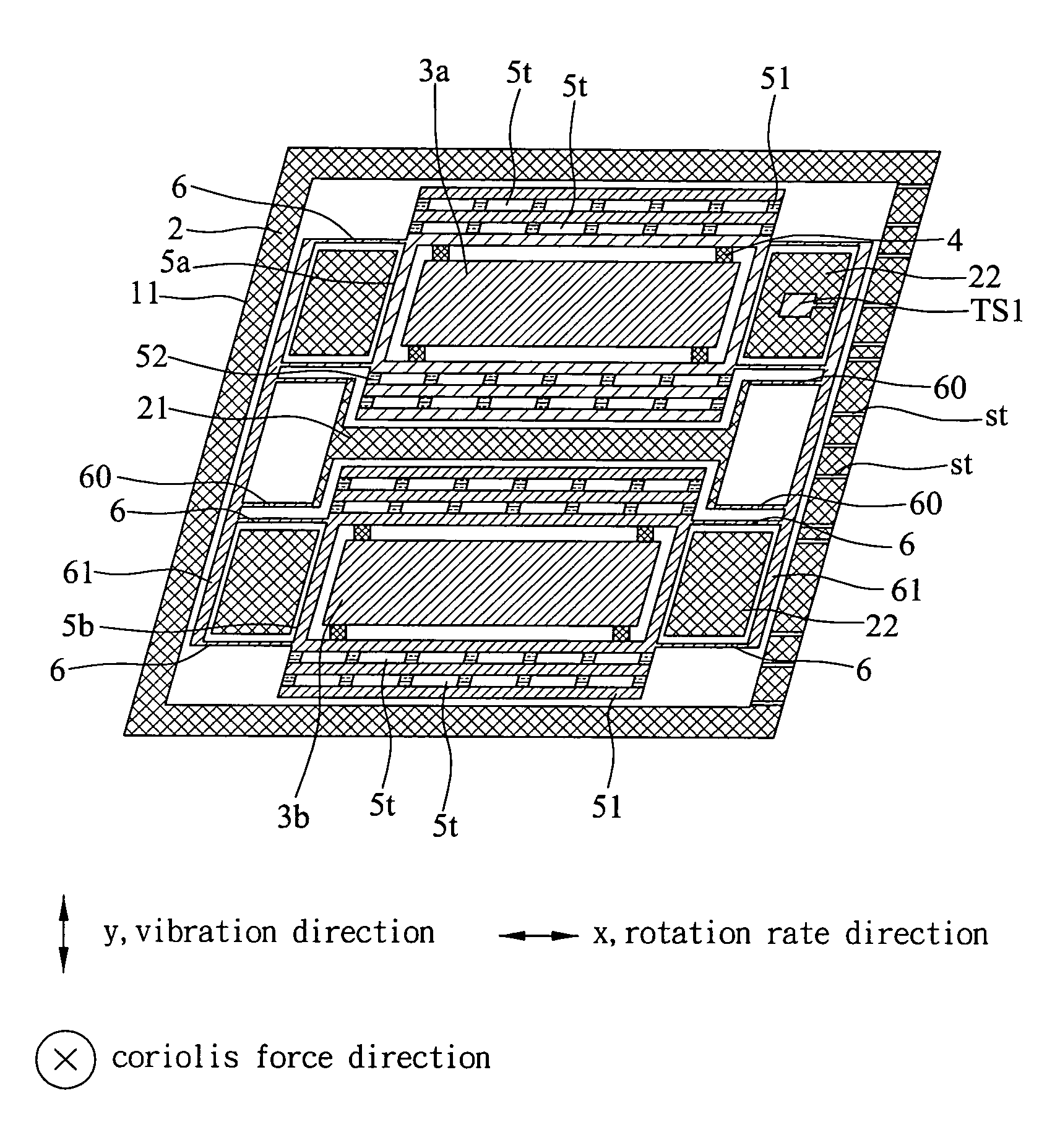
[0016]FIG. 3 shows the top view of a dual inertial sensor in accordance with the present invention. Its structure is made by wet etching a (110) silicon chip 11. It is shaped as a parallelogram, instead of a rectangular shown in FIG. 1. The sides of all the components are in parallel with the intersection line of the (110) silicon chip surface and the silicon lattice {1-1-1} facet or {1-11} facet. Any two sides form an angle of 109.48° or 70.52°; hence most of the components are shaped as parallelograms. Because the two {111} facets, namely {1-1-1} and {1-11}, of the (110) silicon chip are perpendicular to the {110} facet, and conventional KOH and EDP etching solutions etch {111} facet much slower than {100} or {110} facets, a vertical surface can be obtained by keeping the protective mask aligned with the intersection line of the (110) silicon chip surface and the {1-1-1} facet or the {1-11} facet during the etching process. In this embodiment, the structure comprises an outer fram...


PUM


Abstract

A silicon dual inertial sensor made of a (110) silicon chip comprises at least a proof-mass, which is connected to a corresponding inner frame with a plurality of sensing resilient beams to make it easier for the proof-mass to move perpendicular to the surface of the silicon chip (defined as z-axis), and each inner frame is connected to an outer frame with a plurality of driving resilient beams, or connected to common connection beams, which are then connected to a central anchor with common resilient supporting beams to make it easier for the inner frame to move in parallel with the surface of the silicon chip (defined as y-axis). Each inner frame is driven by a driver to move in an opposite direction along the y-axis, and also move the proof-mass in the opposite direction along the y-axis. If there is a rotation rate input along the x-axis, it will generate a Coriolis force to make each proof-mass move in the opposite direction of the z-axis. If an acceleration is input along the z-axis, the specific force will move the proof-masses with the same direction. When the proof-masses move or oscillate, the capacitance of the capacitor formed with sensing electrodes will change due to the change of the distance. The moving distance can be obtained by measuring the change of the capacitance. Because the rotation rate outputs an alternating signal, and the acceleration outputs a direct signal, they can be separated with signal processing. The deep vertical etching characteristics of the (110) silicon chip is utilized to make the driving beam in order to control the driving resonance frequency more precisely, and improve the yield rate and the performance of the gyroscope.

Description

FIELD OF THE INVENTION[0001]The present invention relates to dual inertial sensors made with micro-machining technology, including both functions of a gyroscope (angular rate sensor) and an accelerometer (acceleration sensor), and more particularly to dual inertial sensors made with bulk-micromachining and wet etching on (110) silicon chips.BACKGROUND OF THE INVENTION[0002]A conventional structure of dual inertial sensors made with bulk-micromachining is shown in FIG. 1. It is made of (100) silicon chips 1, comprising an outer frame 2. The outer frame 2 comprises one or more inner frame 5, and each inner frame 5 is further comprising a proof-mass 3. The proof-mass 3 is connected to the inner frame 5 by a plurality of sensing flexible beams 4, and the inner frame 5 is connected to the outer frame 2 by a plurality of driving flexible beams 6. The sensing beams 4 facilitate the proof-mass 3 to move perpendicular to the surface of the silicon chip defined as z-direction), and the drivin...

Claims


Application Information

Patent Timeline
Patent Type & Authority Patents(United States)
IPC IPC(8): G01P15/08G01C19/56G01P15/125
CPCG01C19/5719G01P15/0802G01P15/125
Inventor CHEN, SHYU-MOUTZUOO, SHEAU-SHIKAU, CHUNG-TA
Owner MIN OF NAT DEFENSE
Why Eureka
Try Eureka