A kind of mems device preparation method

A device and component technology, applied in the field of MEMS devices and their preparation, can solve the problems of the decrease of the signal-to-noise ratio and sensitivity of the MEMS microphone, the decrease of the effective stiffness of the MEMS microphone backplane, the decrease of the effective stiffness of the backplane and the backplane, etc. The effect of meeting performance requirements and avoiding resonance

Active Publication Date: 2020-02-11
SEMICON MFG INT (SHANGHAI) CORP
View PDF7 Cites 0 Cited by
  • Summary
  • Abstract
  • Description
  • Claims
  • Application Information

AI Technical Summary

Problems solved by technology

[0005] In order to improve the performance of the MEMS microphone at present, some perforations are usually arranged in the back plate. When the size and size of the perforation in the back plate are certain, the thicker the thickness of the back plate, the greater the air damping, resulting in the signal-to-noise of the MEMS microphone. Ratio and Sensitivity Decrease
If the number or size of perforations in the backplane is increased, the effective stiffness of the MEMS microphone backplane will decrease, and the backplane will easily deform under the action of sound pressure
In addition, reducing the thickness of the backplane also tends to reduce the effective stiffness of the backplane

Method used


Image

  • A kind of mems device preparation method
  • A kind of mems device preparation method
  • A kind of mems device preparation method

Examples


Embodiment 1

[0056] In order to solve the problems existing in the prior art, a MEMS device is provided, and the MEMS device will be further described below in conjunction with the accompanying drawings, wherein Figure 1g A schematic structural diagram of a MEMS device in a specific embodiment of the present invention.

[0057] First, refer to Figure 1g , the MEMS device comprising:

[0058] semiconductor substrate 101;

[0059] A backplane 103, located above the semiconductor substrate, wherein the backplane is provided with several spaced through holes;

[0060] The diaphragm 105 is located above the backboard;

[0061] a sacrificial layer, located between the diaphragm 105 and the back plate 103;

[0062] Wherein, a cavity is formed between the diaphragm 105 and the back plate 103 , and several back cavities are formed in the semiconductor substrate below the cavity.

[0063] The MEMS device described in the present invention is a MEMS microphone.

[0064] In the MEMS microphone...

Embodiment 2

[0082] The present invention also provides a kind of preparation method of described MEMS device, below in conjunction with Figures 1a-1g To further illustrate the method, the above 1a-1g are schematic diagrams of the fabrication process of the MEMS device in this embodiment.

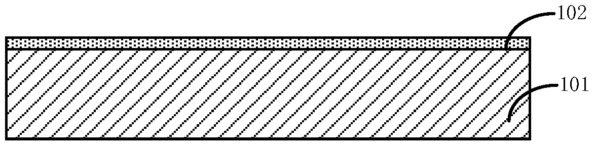
[0083] First, step 201 is performed to provide a semiconductor substrate 101 and form an insulating layer 102 on the semiconductor substrate 101 .

[0084] Specifically, such as Figure 1a As shown, in this step, the semiconductor substrate 101 can be at least one of the materials mentioned below: silicon, silicon-on-insulator (SOI), silicon-on-insulator (SSOI), and germanium-on-insulator Silicon (S-SiGeOI), silicon germanium on insulator (SiGeOI) and germanium on insulator (GeOI), etc.

[0085] Then an insulating layer 102 is formed on the semiconductor substrate 101. Optionally, the insulating layer 102 may be SiN, but not limited to the material.

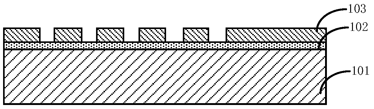
[0086] Step 202 is executed to form a backplane 1...

Embodiment 3

[0130] As an alternative implementation of the present invention, the positions of the back plate and the diaphragm can be interchanged, for example, the diaphragm is located above the semiconductor substrate, and the back plate is located on the side of the diaphragm. Above, several perforations are formed in the diaphragm, and several back cavities exposing the diaphragm are formed in the semiconductor substrate, and the diaphragm is supported by the intervals between the back cavities.

[0131] The MEMS device and the preparation method can refer to Embodiments 1 and 2, except that the positions of the back plate and the diaphragm are exchanged.


PUM


Abstract

The invention relates to an MEMS (Micro Electro Mechanical Systems) device, a manufacturing method thereof and an electronic device. The device comprises a semiconductor substrate, a back plate, a membrane and a sacrificial layer, wherein the back plate is positioned above the semiconductor substrate; a plurality of spaced through holes are formed in the back plate; the membrane is positioned above the back plate; the sacrificial layer is positioned between the membrane and the back plate; a cavity is formed between the membrane and the back plate; and a plurality of spaced back cavities are formed in the semiconductor substrate below the cavity. A design of the plurality of back cavities is adopted, and spaces among the back cavities are used for supporting the back plate, so that the rigidity of the back plate is enhanced; the thickness of the back plate can be reduced to reduce air damping, and the signal-to-noise ratio and the sensitivity of an MEMS microphone are increased. In the design, no process step is added; the process difficulty is not increased; and only etching illumination of the back cavities needs to be changed. The design of the back cavities can be changed flexibly in order to meet the performance requirement of the MEMS microphone.

Description

technical field [0001] The invention relates to the field of semiconductors, in particular, the invention relates to a MEMS device, a preparation method thereof, and an electronic device. Background technique [0002] With the continuous development of semiconductor technology, smart phones, integrated CMOS and micro-electromechanical systems (MEMS) devices have increasingly become the most mainstream and advanced technologies in the market for sensor products, and with technology updates, and Towards small size, high performance and low power consumption. [0003] Among them, MEMS sensors are widely used in automotive electronics: such as TPMS, engine oil pressure sensor, air pressure sensor of automobile brake system, automobile engine intake manifold pressure sensor (TMAP), common rail pressure sensor of diesel engine; consumer electronics: such as tire pressure gauge , sphygmomanometer, cabinet scale, health scale, pressure sensor for washing machine, dishwasher, refrig...

Claims


Application Information

Patent Timeline
Patent Type & Authority Patents(China)
IPC IPC(8): H04R19/04B81B7/02B81C1/00
Inventor 何昭文
Owner SEMICON MFG INT (SHANGHAI) CORP
Why Eureka
Try Eureka