
Bismuth titanium silicon oxide, bismuth titanium silicon oxide thin film, and method for forming the thin film

a technology of titanium silicon oxide and bismuth titanium, which is applied in the direction of chemical vapor deposition coating, natural mineral layered products, water-setting substance layered products, etc., can solve the problems of shortening the life of parts of film formation systems and equipment, and the stability of precursor solutions degrades during storage, so as to achieve simple and easily reproducible methods and good electrical properties

Inactive Publication Date: 2005-07-19
SAMSUNG ELECTRONICS CO LTD
View PDF9 Cites 7 Cited by
  • Summary
  • Abstract
  • Description
  • Claims
  • Application Information

AI Technical Summary

Benefits of technology

[0008]According to another feature of an embodiment of the present invention, there is provided a thin film formed of the above bismuth titanium silicon oxide and a simple and easily reproducible method for forming the bismuth-titanium-silicon oxide thin film.
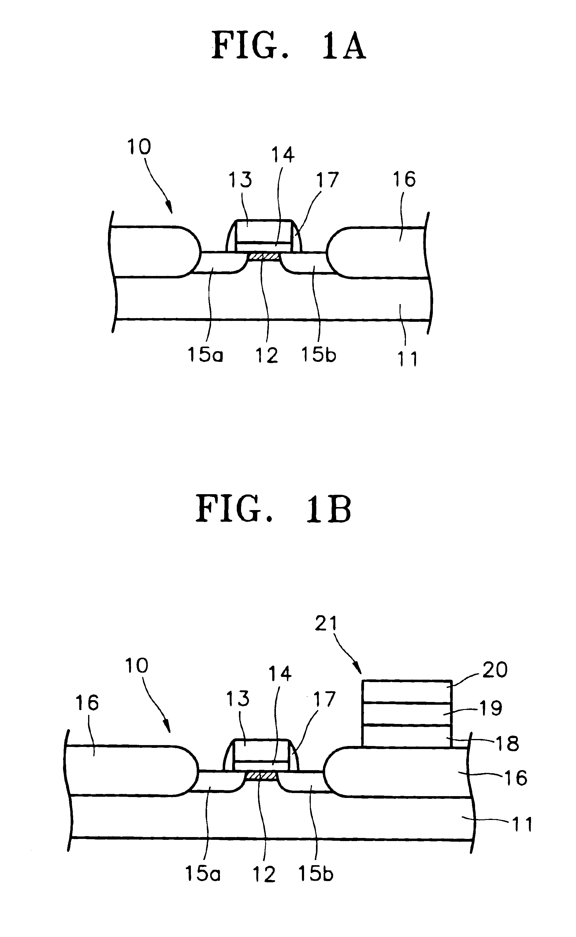
[0009]According to yet another feature of an embodiment of the present invention, there is provided a capacitor and a transistor for semiconductor devices with good electrical properties, which include the bismuth-titanium-silicon oxide thin film, and an electronic device employing the capacitor and / or the transistor.

Problems solved by technology

However, these methods cause problems when applied to form such high dielectric thin films.
However, high temperatures shorten the lifespan of parts of film formation systems and equipment.
Moreover, when a multi-component film is formed using these high dielectric materials, different kinds of precursors mixed in a single cocktail solution interact with one another so that the stability of the precursor solution degrades during storage.

Method used


Image

  • Bismuth titanium silicon oxide, bismuth titanium silicon oxide thin film, and method for forming the thin film
  • Bismuth titanium silicon oxide, bismuth titanium silicon oxide thin film, and method for forming the thin film
  • Bismuth titanium silicon oxide, bismuth titanium silicon oxide thin film, and method for forming the thin film

Examples


example 1

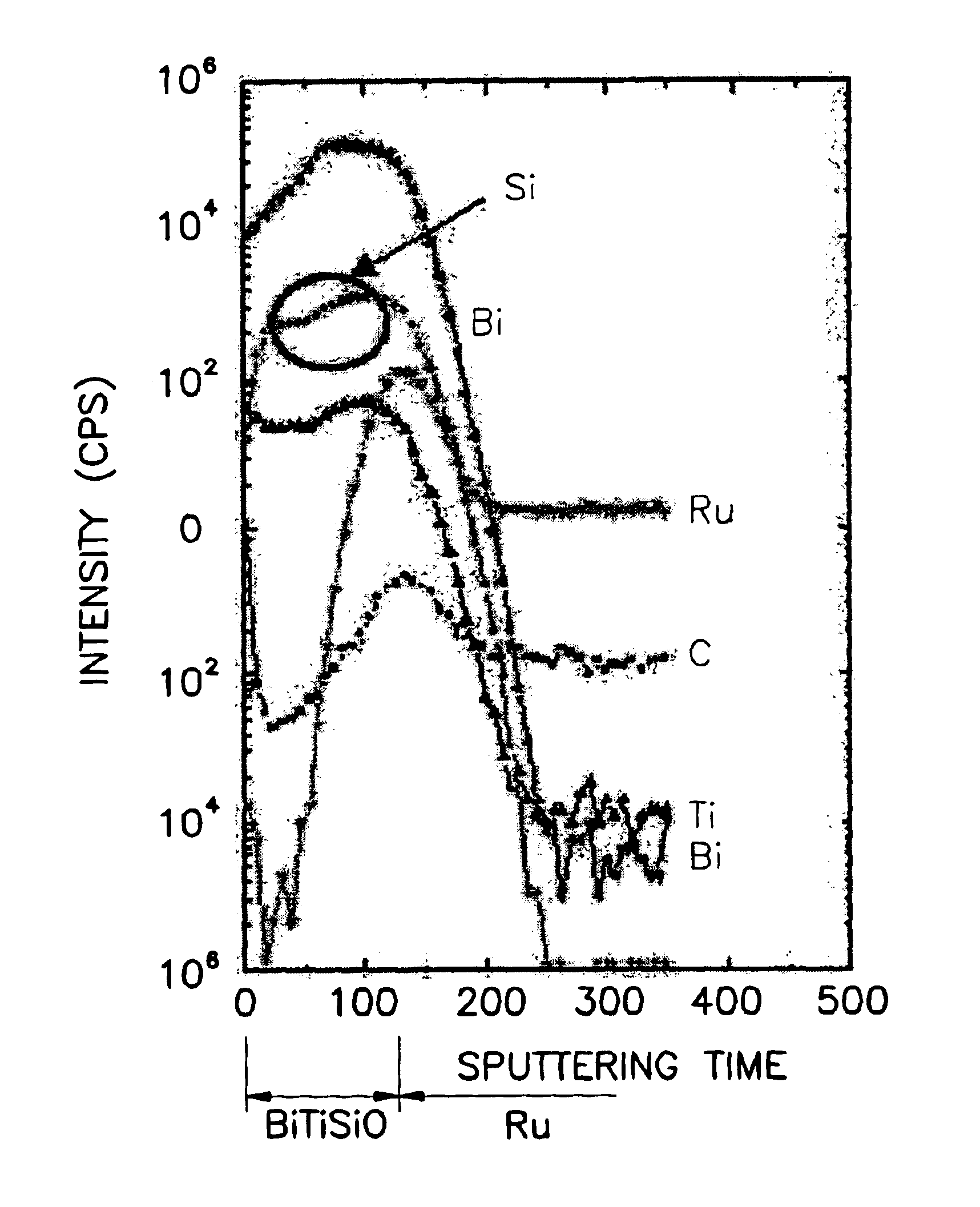
[0070]30 ml of a solution of Bi(MMP)3 (0.4 mol / L) in ethylcyclohexane (ECH), 25 ml of a solution of Ti(MMP)4 (0.4 mol / L) in ECH, and 3.6 ml of tetraethyl orthosilicate (TEOS) were mixed to provide a precursor mixture of a Bi—Ti—Si—O thin film with a concentration of 0.06 mol / L for Bi(MMP)3, 0.05 mol / L for Ti(MMP)4, and 0.08 mol / L for TEOS.

[0071]This precursor mixture was supplied into a vaporizer at 230° C. by direct liquid injection, evaporated by flash evaporation, and carried into a reactor to form a Bi—Ti—Si—O thin film, through atomic deposition, on a Ru / SiO2 / Si substrate whose temperature was maintained at 400° C.

example 2

[0072]25 ml of a solution of Bi(MMP)3 (0.4 mol / L) in ECH, 30 ml of a solution of Ti(MMP)4 (0.4 mol / L) in ECH, and 3.6 ml of TEOS were mixed to provide a precursor mixture of a Bi—Ti—Si—O thin film with a concentration of 0.05 mol / L for Bi(MMP)3, 0.06 mol / L for Ti(MMP)4, and 0.08 mol / L for TEOS.

[0073]This precursor mixture was supplied into a vaporizer at 230° C. by direct liquid injection, evaporated by flash evaporation, and carried into a reactor to form a Bi—Ti—Si—O thin film, through atomic deposition, on a Ru / SiO2 / Si substrate whose temperature was maintained at 400° C.

[0074]In this embodiment, the Bi—Ti—Si—O thin film was formed in the same manner as in Example 1, except that the concentrations of Bi(MMP)3, Ti(MMP)4, and TEOS in ECH in the precursor mixture were varied to 0.05 mol / L, 0.06 mol / L, and 0.08 mol / L, respectively.

example 3

[0075]25 ml of a solution of Bi(MMP)3 (0.4 mol / L) in ECH, 25 ml of a solution of Ti(MMP)4 (0.4 mol / L) in ECH, and 4 ml of TEOS were mixed to provide a precursor mixture of a Bi—Ti—Si—O thin film with a concentration of 0.05 mol / L for Bi(MMP)3, 0.05 mol / L for Ti(MMP)4, and 0.09 mol / L for TEOS.

[0076]This precursor mixture was supplied into a vaporizer at 230° C. by direct liquid injection, evaporated by flash evaporation, and carried into a reactor to form a Bi—Ti—Si—O thin film, through atomic deposition, on a Ru / SiO2 / Si substrate whose temperature was maintained at 400° C.

[0077]In this embodiment, the Bi—Ti—Si—O thin film was formed in the same manner as in Example 1, except that the concentrations of Bi(MMP)3, Ti(MMP)4, and TEOS in ECH in the precursor mixture were varied to 0.05 mol / L, 0.05 mol / L, and 0.09 mol / L, respectively.

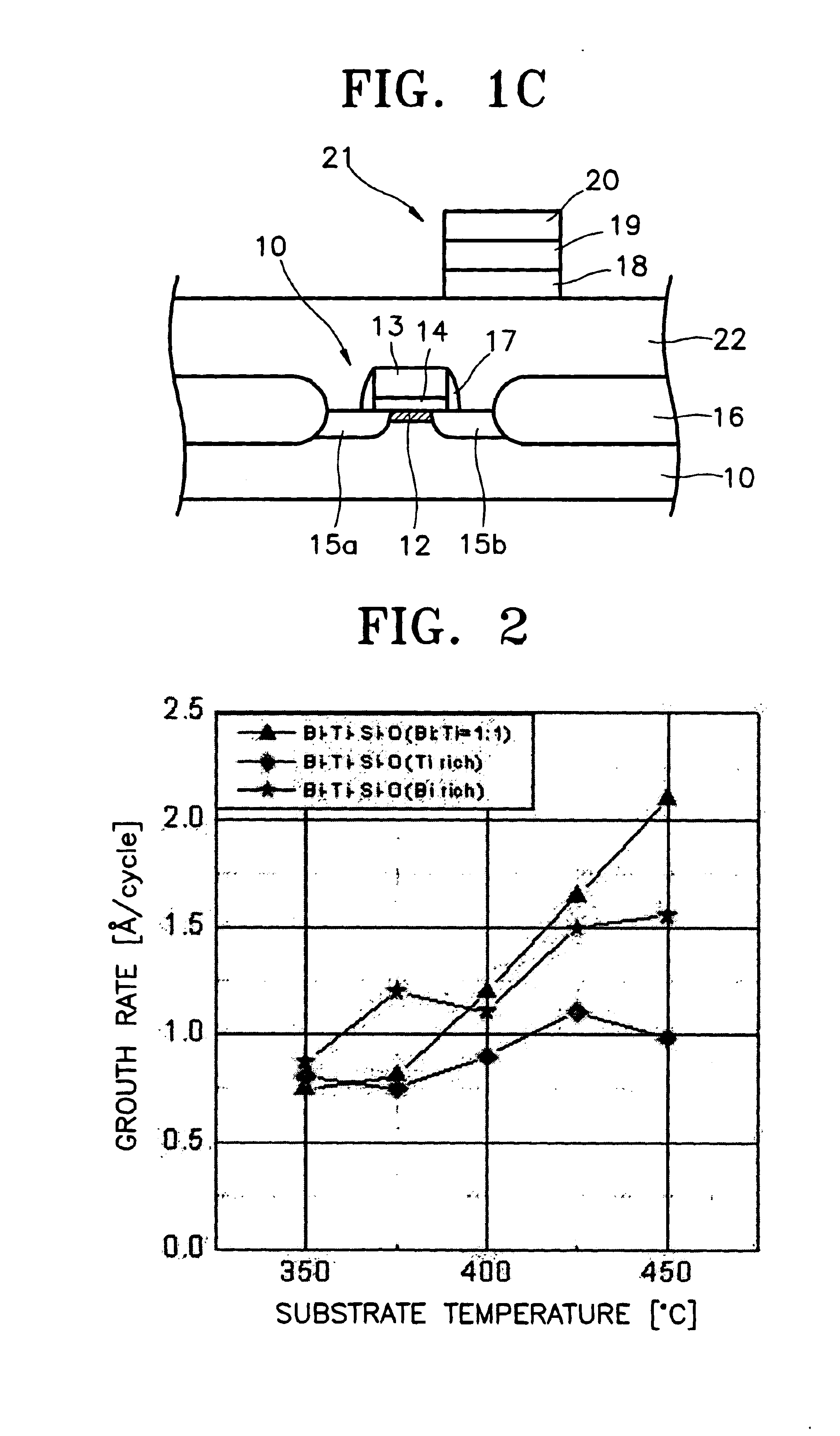
[0078]The growth rate of a bi—TI—Si—O thin film at various substrate temperatures was measured using the Bi—Ti—Si—O thin films formed in Examples 1 through 3...


PUM

PropertyMeasurementUnit
dielectric constantaaaaaaaaaa
temperatureaaaaaaaaaa

Abstract

A bismuth titanium silicon oxide having a pyrochlore phase, a thin film formed of the bismuth titanium silicon oxide, a method for forming the bismuth-titanium-silicon oxide thin film, a capacitor and a transistor for a semiconductor device including the bismuth-titanium-silicon oxide thin film, and an electronic device employing the capacitor and / or the transistor are provided. The bismuth titanium silicon oxide has good dielectric properties and is thermally and chemically stable. The bismuth-titanium-silicon oxide thin film can be effectively used as a dielectric film of a capacitor or as a gate dielectric film of a transistor in a semiconductor device. Various electronic devices having good electrical properties can be manufactured using the capacitor and / or the transistor having the bismuth-titanium-silicon oxide film.

Description

BACKGROUND OF THE INVENTION[0001]1. Field of the Invention[0002]The present invention relates to a titanium silicon oxide, a titanium silicon oxide thin film, and a method for forming the titanium silicon oxide thin film. More particularly, the present invention is directed to a novel bismuth titanium silicon oxide, a thin film formed of the bismuth titanium silicon oxide, a method for forming the bismuth-titanium-silicon oxide thin film, a capacitor and a transistor using the bismuth-titanium-silicon oxide thin film, and an electronic device having the capacitor and / or the transistor. The novel bismuth titanium silicon oxide exhibits good dielectric properties that enables it to be used in a capacitor and a transistor in highly integrated memory devices.[0003]2. Description of the Related Art[0004]As the integration density of memory devices become greater, unit cell size and capacitor area become smaller. Accordingly, there have been many attempts to use a high dielectric constant...

Claims


Application Information

Patent Timeline
Patent Type & Authority Patents(United States)
IPC IPC(8): C04B35/475C04B35/462C01G29/00H01L21/28H01L21/02H01L29/51H01L21/316H01L29/40C01B33/00C23C14/06C23C16/42H10B12/00
CPCC01G29/006C04B35/16C04B35/475C04B35/6264H01L21/28185H01L21/28194H01L21/31691H01L29/516H01L29/517C01P2002/36C01P2002/72C01P2002/77C01P2002/85C01P2002/89C01P2004/03C01P2004/04C01P2004/80C01P2006/40C04B2235/3232C04B2235/3298C04B2235/3418C04B2235/441C04B2235/444C04B2235/658C04B2235/6581C04B2235/76H01L28/55H01L21/02205H01L21/02216H01L21/02161H01L21/02153H01L21/02271H01L21/02211H01L21/02197H01L21/02194H01L21/02164H01L21/02255H01L21/0228H01L2924/01083H01L2924/01022H10B12/00H01L21/02337
Inventor CHO, YOUNG-JINMIN, YO-SEPPARK, YOUNG-SOOLEE, JUNG-HYUNLEE, JUNE-KEYLEE, YONG-KYUN
Owner SAMSUNG ELECTRONICS CO LTD
Learn More