Semiconductor device having a high-dielectric gate insulation film and fabrication process thereof
a technology of silicon oxide and gate insulation film, which is applied in the direction of semiconductor/solid-state device details, coatings, transistors, etc., can solve the problems of increased direct tunnel current, abnormal operation, and higher power consumption of conventional gate insulation film of silicon oxid
- Summary
- Abstract
- Description
- Claims
- Application Information
AI Technical Summary
Benefits of technology
Problems solved by technology
Method used
Image

Examples
third embodiment
[The Third Embodiment]
[0087]FIG. 6 shows a structure of a CMOS semiconductor device 20 of a third embodiment of the present invention.
[0088]With reference to FIG. 6, the CMOS semiconductor device 20 includes an isolation area 22 that divides a p-type Si substrate 21 into a p-channel MOS area 20A and an n-channel MOS area 20B. In the p-channel MOS area 20A, an n-type well 20W is formed.
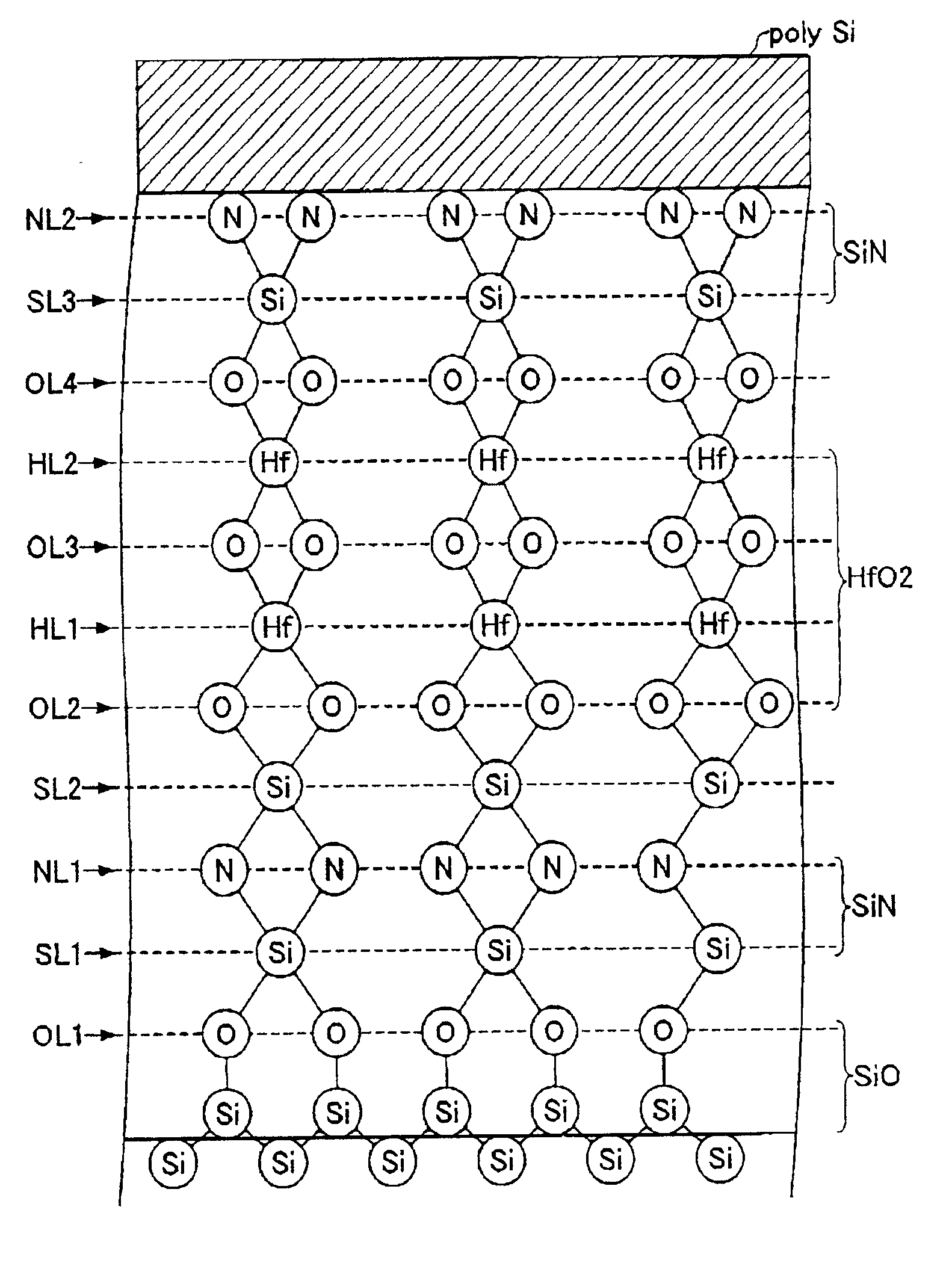
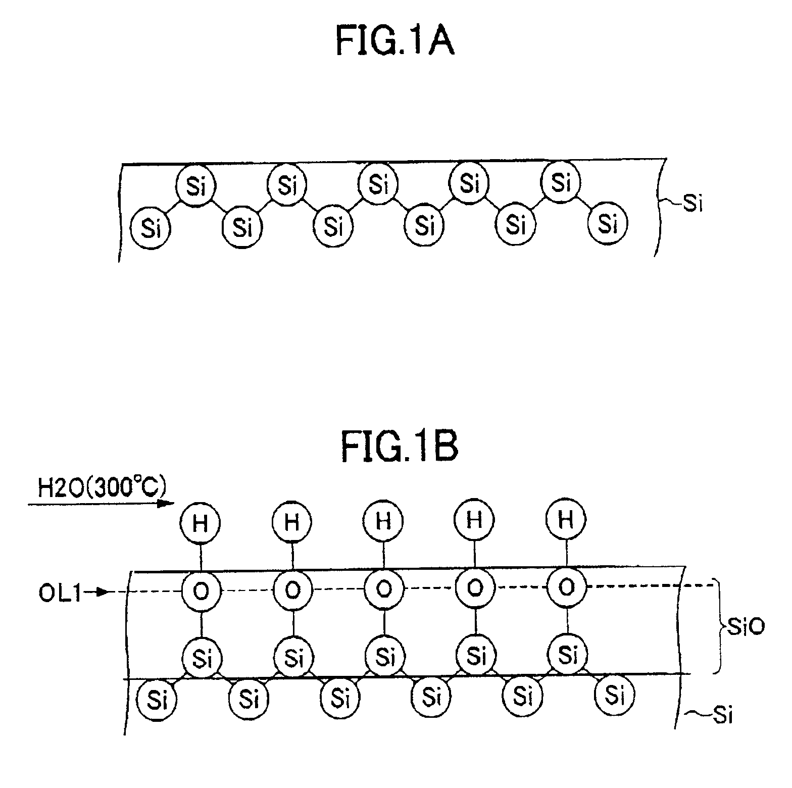
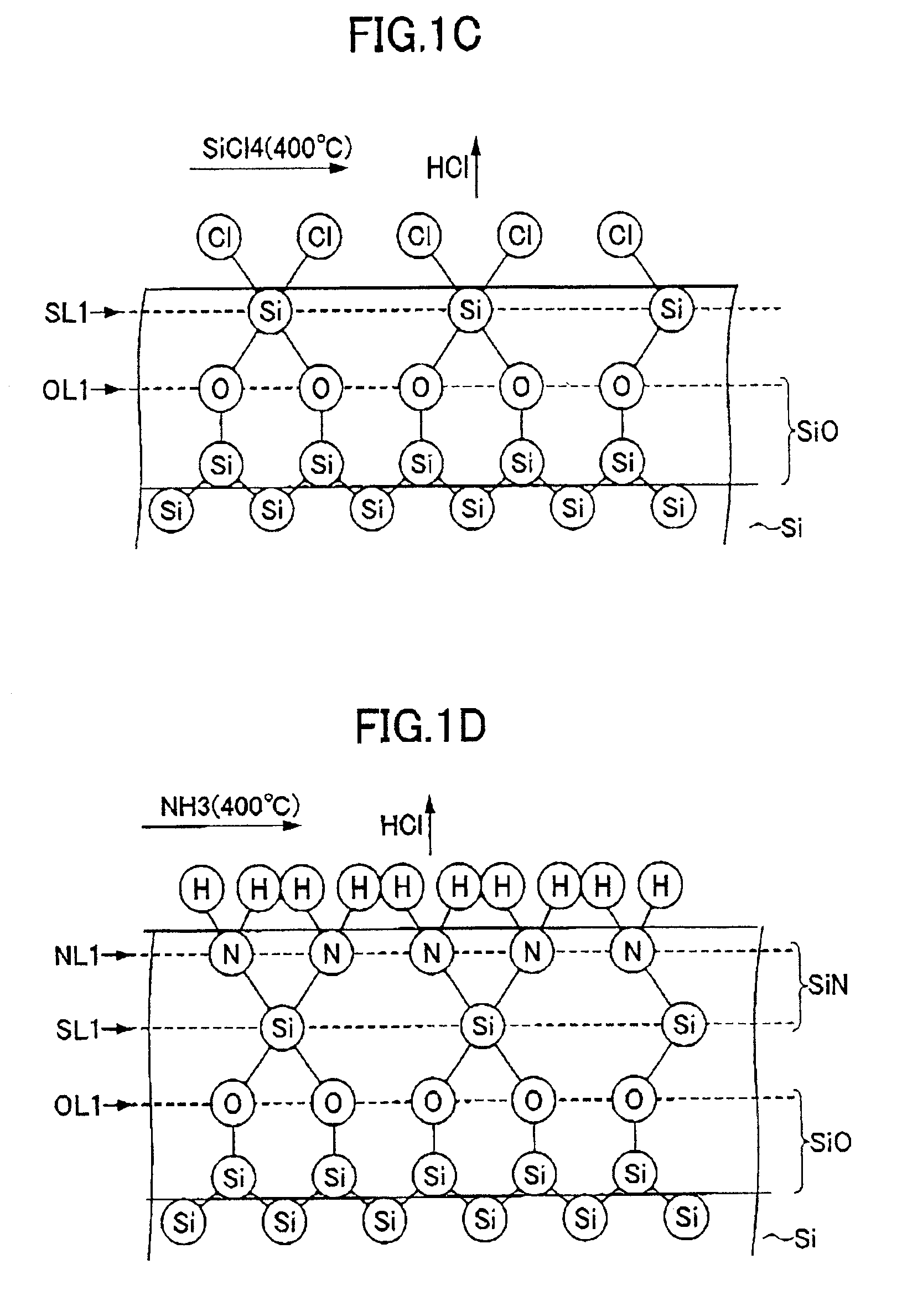
[0089]In the p-channel MOS area 20A, a high-K dielectric gate insulation film 23A that has the same layer structure as shown in FIG. 1J is formed, corresponding to the channel region, and a poly silicon gate electrode 24A doped by B is formed on the gate insulation film 23A. Further, on the poly silicon gate electrode 24A, a silicide layer 25A is formed by the salicide process. Further, a sidewall film is formed on the both sides of the poly silicon gate electrode 24A.
[0090]In the p-channel MOS area 20A, a p-type LDO area 26Lp is formed corresponding to each side of the surface of the wall of the gate ...
PUM
| Property | Measurement | Unit |
|---|---|---|
| thickness | aaaaa | aaaaa |
| specific dielectric constant | aaaaa | aaaaa |
| gate length | aaaaa | aaaaa |
Abstract
Description
Claims
Application Information
 - R&D
- Intellectual Property
- Life Sciences
- Materials
- Tech Scout
- Unparalleled Data Quality
- Higher Quality Content
- 60% Fewer Hallucinations
Browse by: Latest US Patents, China's latest patents, Technical Efficacy Thesaurus, Application Domain, Technology Topic, Popular Technical Reports.
© 2025 PatSnap. All rights reserved.Legal|Privacy policy|Modern Slavery Act Transparency Statement|Sitemap|About US| Contact US: help@patsnap.com