Large area orientation of block copolymer microdomains in thin films
a copolymer microdomain and thin film technology, applied in the direction of instruments, applications, ways, etc., can solve the problems of difficult control, time-consuming cases, and/or inability to form patterns,
- Summary
- Abstract
- Description
- Claims
- Application Information
AI Technical Summary
Benefits of technology
Problems solved by technology
Method used
Image
Examples
example 1
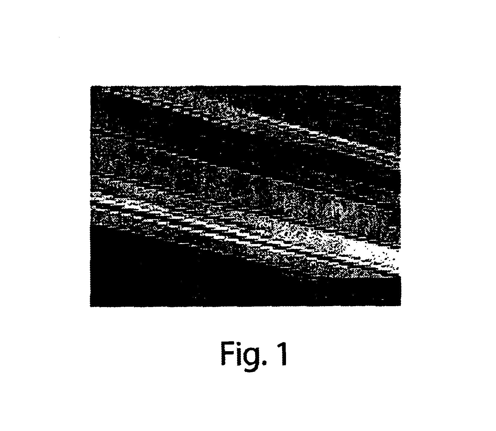
[0060]A polystyrene-block-poly(methyl methacrylate), PS / PMMA (26 / 32), diblock copolymer and a polystyrene-block-polyisoprene diblock copolymer, PS / PI(45 / 12) were used. The PS / PMMA-(26 / 32) sample had a total molecular weight of 58,500 g / mol, a polydispersity of 1.06, with PS and PMMA blocks of 26,000 and 32,000 g / mol, respectively. This sample had a bulk lamellar microstructure (evidenced by small-angle X-ray scattering (SAXS): d100lam≈39 nm, consistent with the 49% volume fraction of the PS block. The PS / PI(45 / 12) sample had a total molecular weight of 57,000 g / mol with PS and PI blocks of 45,000 and 12,000 g / mol, respectively. Because the volume fraction of the PI block was 24%, the bulk sample had a hexagonally packed cylindrical microstructure of the minority PI component (evidenced by SAXS: d1010cyl≈42 nm). The PS / PMMA(26 / 32) was purchased from Polymer Laboratories, while the PS / PI(45 / 12) block copolymer was supplied by Exxon Research and Engineering. The processing method was b...
example 2
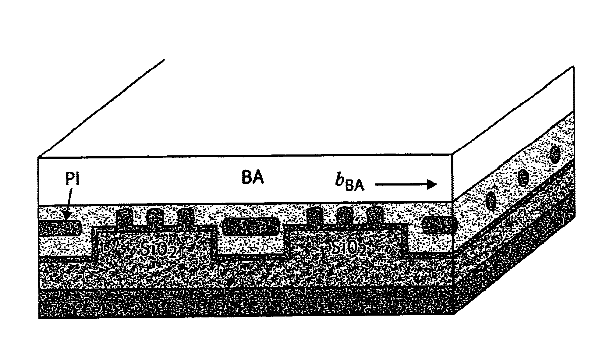
[0074]A polystyrene-block-polyisoprene diblock copolymer, denoted PS / PI(45 / 12) having a PS block of 45,000 g / mol and a PI block of 12,000 g / mol was used. The copolymer has a bulk microdomain structure that had hexagonally packed, cylindrical PI domains with an intercylinder distance (d0) of 48 nm and cylinder diameters of 20 nm. The block copolymer was supplied by Exxon / Mobil Research.
[0075]The patterned substrate was produced via standard lithographic techniques. The substrate pattern had 30 nm high, 2 micron×2 micron square mesas arranged in a square array with a 4 micron spacing as shown in the schematic diagram of FIG. 6a. The square-shaped mesas are made by selective etching of a thermally grown silicon oxide on a 4 inch wafer.
[0076]The topography of the patterned substrate produced thickness variations in the directionally solidified block copolymer thin films. It is believed that the thickness variations resulted from the copolymer confinement between the flat BA single cryst...
example 3
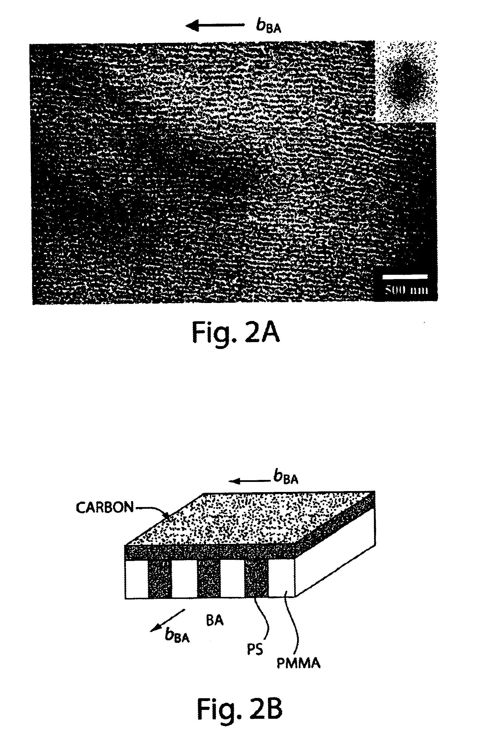
[0084]A polystyrene-block-polyethlylene (PS / PE) diblock copolymer, which was prepared by hydrogenation of polystyrene-block-1,4-butadiene, previously synthesized via sequential anionic polymerization as described by Morton et al. in Anionic polymerization of vinyl monomers, J. Rubber Chem. Tech. 48, 359 (1975) was used. The amorphous PS block and the crystallizable PE block had molecular weights of 40,000 and 10,000 g / mol respectively. The volume fraction of the PE block was 0.24 with a melting point of 98° C. Near the eutectic temperature, the block copolymer is in the intermediate segregation regime. SAXS of bulk films of PS / PE showed multiple low angle reflections characteristic of hexagonally packed cylinders with the first Bragg peak at q=0.15 nm−1 corresponding to a cylinder-cylinder spacing of 42 nm.
[0085]When cast from dilute xylene solution (0.3 wt %) onto an amorphous carbon support film, the structure consisted of in-plane meandering cylinders of PE in the PS matrix as sh...
PUM
| Property | Measurement | Unit |
|---|---|---|
| Melting point | aaaaa | aaaaa |
| Melting point | aaaaa | aaaaa |
| Melting point | aaaaa | aaaaa |
Abstract
Description
Claims
Application Information
 - R&D
- Intellectual Property
- Life Sciences
- Materials
- Tech Scout
- Unparalleled Data Quality
- Higher Quality Content
- 60% Fewer Hallucinations
Browse by: Latest US Patents, China's latest patents, Technical Efficacy Thesaurus, Application Domain, Technology Topic, Popular Technical Reports.
© 2025 PatSnap. All rights reserved.Legal|Privacy policy|Modern Slavery Act Transparency Statement|Sitemap|About US| Contact US: help@patsnap.com


