
Method of depositing dielectric materials in damascene applications

a technology of dielectric materials and damascene, which is applied in the direction of chemical vapor deposition coating, semiconductor/solid-state device details, coatings, etc., can solve the problems of copper etching and achieving a precise pattern, copper is difficult to etch and achieve, and the traditional process of etching/deposition of copper for forming interconnects has not been satisfactory. , the formation of short-circuits and the effect of device failur

Inactive Publication Date: 2005-05-10
APPLIED MATERIALS INC
View PDF74 Cites 93 Cited by
  • Summary
  • Abstract
  • Description
  • Claims
  • Application Information

AI Technical Summary

Benefits of technology

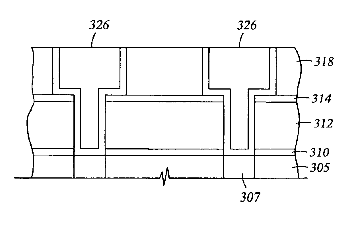
The invention provides methods for depositing layers of oxygen-doped silicon carbide with low dielectric constants. These methods involve reacting a processing gas containing oxygen and carbon with an oxygen-free organosilicon compound to deposit a dielectric material on a substrate. The dielectric material contains silicon, oxygen, and carbon, with an oxygen content of about 15 atomic percent or less. The methods also involve depositing a barrier layer on the substrate, and then depositing an intermetal dielectric layer on the barrier layer. Additionally, the methods involve depositing a hardmask layer on the at least one dielectric layer, patterning the hardmask layer, and depositing a conductive material in the patterned areas. The polishing process has a removal rate ratio between the conductive material and the hardmask layer of about 4:1 or greater. The technical effects of the invention include improved performance and reliability of semiconductor devices, reduced signal delay, and reduced power consumption.

Problems solved by technology

One difficulty in using copper in semiconductor devices is that copper is difficult to etch and achieve a precise pattern.
Etching with copper using traditional deposition / etch processes for forming interconnects has been less than satisfactory.
However, low k dielectric materials are often porous and susceptible to interlayer diffusion of conductive materials, such as copper, which can result in the formation of short-circuits and device failure.
Additionally, low k materials are susceptible to surface defects or feature deformation during polishing and removal of conductive materials under conventional polishing processes.
One difficulty when using hardmasks is that conventional hardmask materials do not have sufficient resistivity to polishing, which may result in premature removal of the hardmask and expose the underlying material to the process.
The exposed underlying material, such as the low k dielectric material, may be damaged and result in surface defects and feature deformation.
Current hardmask materials have not satisfactorily produced both low k material and sufficient polishing resistivity to be used in damascene fabrication.

Method used


Image

  • Method of depositing dielectric materials in damascene applications
  • Method of depositing dielectric materials in damascene applications
  • Method of depositing dielectric materials in damascene applications

Examples


examples

[0080]Organosilicon compounds described herein were deposited as barrier layers on substrate surface and analyzed. In one example, a silicon carbide film was deposited from a mixed precursor processing gas containing an oxygen-containing organosilicon precursor and an oxygen-free organosilicon compound and compared to a silicon carbide film from a conventional silicon carbide precursor, trimethylsilane.

[0081]An oxygen-doped silicon carbide barrier layer was deposited by a mixed precursor process including introducing 1,3,5,7-tetramethylcyclotetrasiloxane (TMCTS) at about 300 mgm into the processing chamber, introducing trimethylsiloxane (TMS) at about 360 mgm into the processing chamber, introducing helium at about 1000 sccm into the processing chamber, generating a plasma in the processing chamber by applying 950 watts of RF energy, maintaining the substrate temperature at about 350° C., maintaining the chamber pressure at about between about 8.7 Torr to deposit an oxygen-doped sil...


PUM

PropertyMeasurementUnit
pressureaaaaaaaaaa
pressureaaaaaaaaaa
temperatureaaaaaaaaaa

Abstract

Methods are provided for depositing an oxygen-doped dielectric layer. The oxygen-doped dielectric layer may be used for a barrier layer or a hardmask. In one aspect, a method is provided for processing a substrate including positioning the substrate in a processing chamber, introducing a processing gas comprising an oxygen-containing organosilicon compound, carbon dioxide, or combinations thereof, and an oxygen-free organosilicon compound to the processing chamber, and reacting the processing gas to deposit an oxygen-doped dielectric material on the substrate, wherein the dielectric material has an oxygen content of about 15 atomic percent or less. The oxygen-doped dielectric material may be used as a barrier layer in damascene or dual damascene applications.

Description

CROSS-REFERENCE TO RELATED APPLICATIONS[0001]This application claims benefit of U.S. provisional Patent Application Ser. No. 60 / 340,615, filed Dec. 14, 2001, which is herein incorporated by reference.BACKGROUND OF THE DISCLOSURE[0002]1. Field of the Invention[0003]The invention relates to the fabrication of integrated circuits and to a process for depositing dielectric layers on a substrate and the structures formed by the dielectric layers.[0004]2. Description of the Related Art[0005]One of the primary steps in the fabrication of modern semiconductor devices is the formation of metal and dielectric layers on a substrate by chemical reaction of gases. Such deposition processes are referred to as chemical vapor deposition or CVD. Conventional CVD processes supply reactive gases to the substrate surface where heat-induced or energy-enhanced chemical reactions take place to produce a desired layer.[0006]Semiconductor device geometries have dramatically decreased in size since such devi...

Claims


Application Information

Patent Timeline
Patent Type & Authority Patents(United States)
IPC IPC(8): C23C16/30C23C16/56C23C16/40H01L21/02H01L21/70H01L21/768H01L21/316H01L21/312H01L21/311C23C16/42H01L23/522
CPCC23C16/30H01L21/76834C23C16/56H01L21/02126H01L21/02211H01L21/02216H01L21/02274H01L21/02304H01L21/3122H01L21/31633H01L21/7681H01L21/76826H01L21/76828H01L21/76829C23C16/401H01L21/31138H01L21/31144H01L21/312H01L21/3127H01L21/76807H01L21/02167H01L21/0212
Inventor LEE, JU-HYUNGXU, PINGVENKATARAMAN, SHANKARXIA, LI-QUNHAN, FEIYIEH, ELLIENEMANI, SRINIVAS D.YIM, KANGSUBMOGHADAM, FARHAD K.SINHA, ASHOK K.ZHENG, YI
Owner APPLIED MATERIALS INC
Learn More