
High density and high programming efficiency MRAM design

a programming efficiency and high density technology, applied in the field of magnetic memories, can solve the problems of the magnetic properties of the portions of soft cladding layers b>1002, /b> and b>1202, > on the vertical sidewalls of conventional lines, and achieve the effect of improving reliability and simplifying fabrication

Inactive Publication Date: 2005-03-08
APPLIED SPINE TECH
View PDF10 Cites 51 Cited by
  • Summary
  • Abstract
  • Description
  • Claims
  • Application Information

AI Technical Summary

Benefits of technology

According to the system and method disclosed herein, the present invention provides a magnetic memory that may be scaled to higher densities, written at relatively low currents, have improved reliability against electromigration, and be simpler to fabricate.

Problems solved by technology

Although this approach works well theoretically, one of ordinary skill in the art will readily recognize that the magnetic properties of the portions of the soft cladding layers 1002 and 1202 on the vertical sidewalls of the conventional lines 10′ and 12′, respectively, are hard to control.
Furthermore, none of the processes can be shared with other CMOS processes.
This complicated fabrication methods pose significant challenge to scaling to higher densities.
As the line width decreases to increase the memory density, the electromigration current density limit poses severe challenges for scaling.
But such conventional methods compromise performance by reducing the speed of the memory and add complexities.
This adversely affects the performance of the overall memory array.
However, the other problems described above, such as the electromigration are still not overcome.

Method used


Image

  • High density and high programming efficiency MRAM design
  • High density and high programming efficiency MRAM design
  • High density and high programming efficiency MRAM design

Examples


Embodiment Construction

The present invention relates to an improvement in magnetic memories. The following description is presented to enable one of ordinary skill in the art to make and use the invention and is provided in the context of a patent application and its requirements. Various modifications to the preferred embodiment will be readily apparent to those skilled in the art and the generic principles herein may be applied to other embodiments. Thus, the present invention is not intended to be limited to the embodiment shown, but is to be accorded the widest scope consistent with the principles and features described herein.

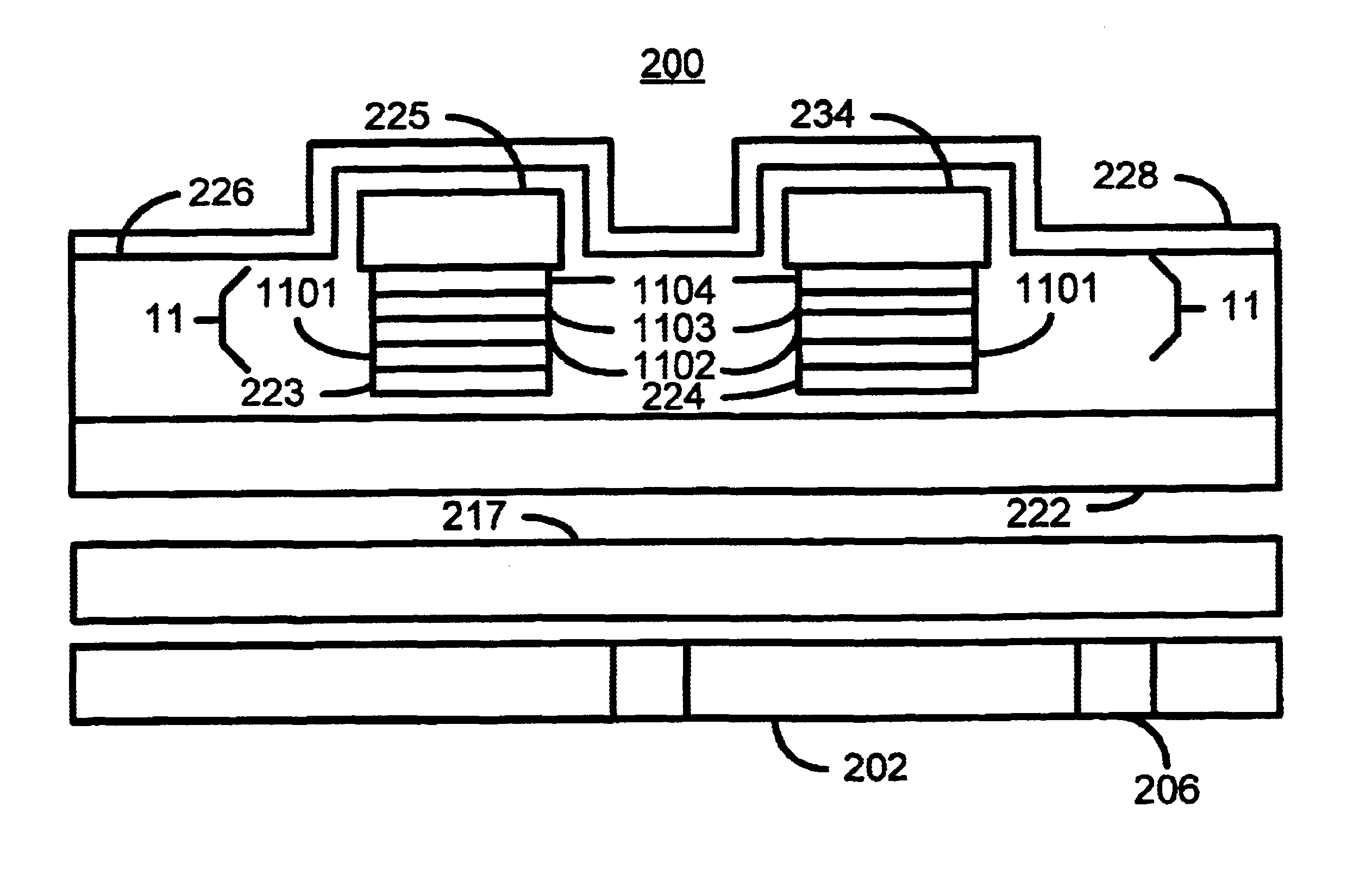
Co-pending U.S. patent application Ser. No. 60 / 431,742 entitled “MRAM MEMORIES UTILIZING MAGNETIC WRITE LINES” assigned to the assignee of the present application describes a MRAM architecture that addresses many of the issues encountered in conventional MRAM deices. Applicant hereby incorporates by reference the above-identified co-pending application. FIG. 3 depicts one embodi...


PUM


Abstract

A method and system for providing a magnetic memory is disclosed. The magnetic memory includes a magnetic element. The magnetic element is written using a first write line and a second write line and resides at an intersection between the first and second write lines. The second write line is oriented at an angle to the first write line. The second write line has a top and at least one side. At least a portion of the second write line is covered by an insulating layer. A magnetic layer covers a portion of the insulating layer. The portion of the insulating layer resides between the magnetic layer and the second write line. The magnetic layer includes a soft magnetic material.

Description

FIELD OF THE INVENTIONThe present invention pertains to magnetic memories, and more particularly to a method and system for providing write lines for nonvolatile magnetic random access memory (MRAM) that may reduce the cell size, simplify fabrication processes, improve reliability, and improve programming efficiency.BACKGROUND OF THE INVENTIONRecently, a renewed interest in thin-film magnetic random access memories (MRAM) has been sparked by the potential application of MRAM to both nonvolatile and volatile memories. FIG. 1 depicts a portion of a conventional MRAM 1. The conventional MRAM includes conventional orthogonal conductor lines 10 and 12, conventional magnetic storage cell 11 and conventional transistor 13. The conventional MRAM 1 utilizes a conventional magnetic tunneling junction (MTJ) stack 11 as a memory cell. Use of a conventional MTJ stack 11 makes it possible to design an MRAM cell with high integration density, high speed, low read power, and soft error rate (SER) i...

Claims


Application Information

Patent Timeline
Patent Type & Authority Patents(United States)
IPC IPC(8): H01L29/66H01L43/00H01L29/82H01L31/062H01L31/06G11CH10B20/00
CPCH01L27/228B82Y10/00H10B61/22
Inventor TSANG, DAVID
Owner APPLIED SPINE TECH
Learn More