Eureka AIR delivers breakthrough ideas for toughest innovation challenges, trusted by R&D personnel around the world.

Method for the production of optical components with increased stability, components obtained thereby and their use

a technology of optical components and stability, applied in the field of optical component production, can solve the problems of unloading of stresses and strains in the material, adversely affecting the power of the material, and additional micro-disruptions in the molecular structure of the base material, so as to increase the yield of such production processes, increase the stability of such components, and reduce the effect of micro-roughness

Inactive Publication Date: 2005-02-15
CARL ZEISS SMT GMBH
View PDF8 Cites 1 Cited by
  • Summary
  • Abstract
  • Description
  • Claims
  • Application Information

AI Technical Summary

Benefits of technology

The invention is a method for producing optical components with a high yield and stability. It involves modeling the component in the desired shape, applying a covering layer, and adjusting the fit accuracy through abrasion of the covering layer. The method reduces the number of processing steps and mechanical stress on the lens. It also reduces micro-roughness and light scatter, and achieves a good fit accuracy. The covering layer can be applied using various techniques, such as ion-beam deposition. The optical component is tempered prior to applying the covering layer to break down strains caused by defects in the crystal structure. The method is particularly useful for producing optical lenses made of crystal materials.

Problems solved by technology

In this way, a light scatter arises, which is typical for each optical component or lens and which adversely affects its power.
In addition to the already present crystal or material defects, this stress leads to additional micro-disruptions in the molecular structure of the base material or leads to unloading of stresses and strains in the material, which are caused, e.g., by crystal defects that are already present.
If the material has crystalline structures and particularly if it is a single crystal, then it may happen that the crystal is disrupted by slight temperature stress or mechanical loads or shifts in fits and starts along a crystal surface to break down the stresses or strains present in the crystal unit.
By the processing of such materials, particularly by grinding and polishing, crystal defects reach the surface due to the abrasion of material associated therewith, so that these crystal defects can unload their stress or strain with a release of energy, which leads to the previously described shift or even to the breaking off of pieces of material of variable size.
Foreign atoms introduce defects in highly pure crystals, because their inappropriate size for the most part gives rise to small glassy regions.
The above-described material defects bring about a further reduction in yield in the production of optical components.
If one additionally considers the reduced yields for large-scale technological processes, in any case, in the growing of large, highly homogeneous, oriented single crystals, as are necessary for optical components with a large diameter, such as, for example, in objectives for microlithography, then an increase in the number of discards during processing or production of such optical components leads to an additional enormous reduction in the yield of the total process, which greatly increases costs.
It has now been found in crystals that by polishing to a small micro-roughness in an attempt to prevent light scatter, a good fit cannot be achieved.
On the other hand, if it is attempted to obtain a good fit by intense polishing, then an intensified micro-roughness of the surface occurs and thus there are considerable losses due to light scatter.

Method used

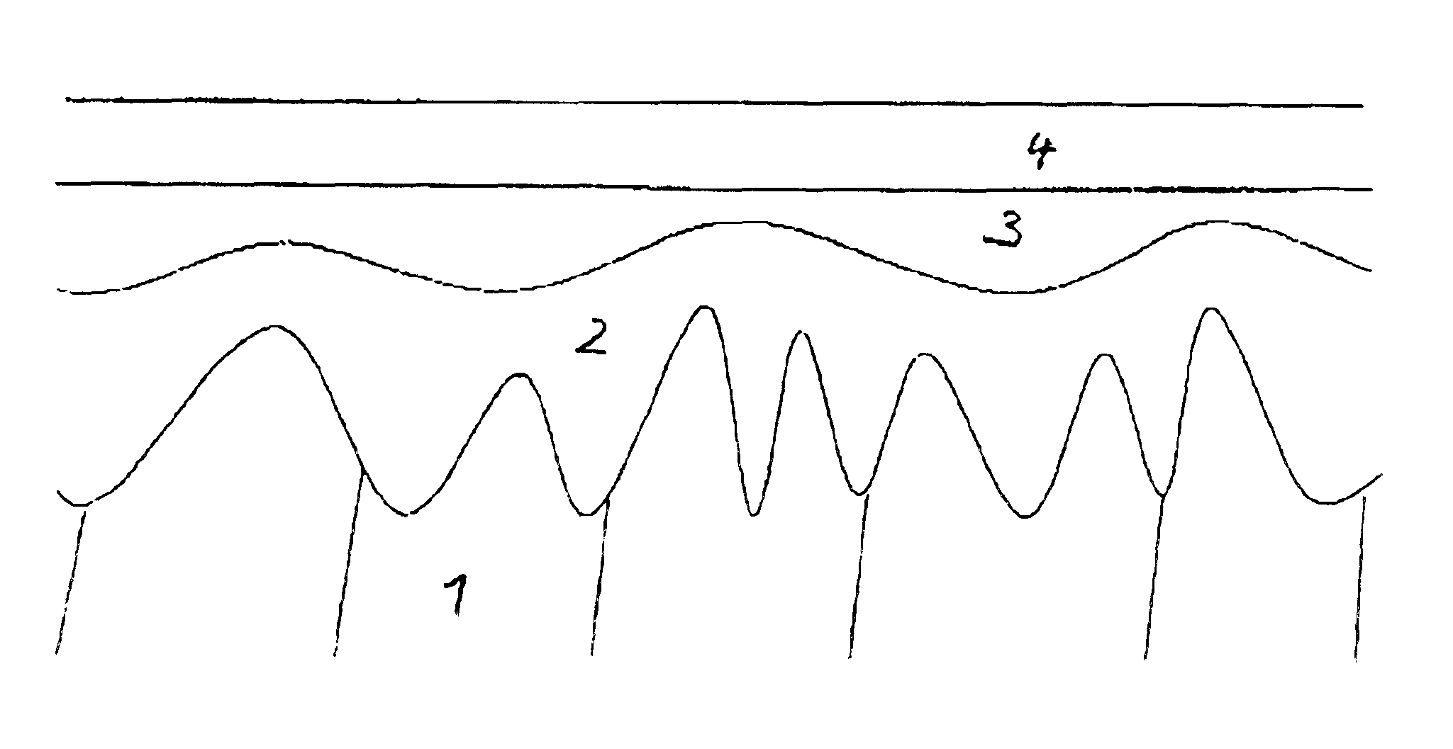
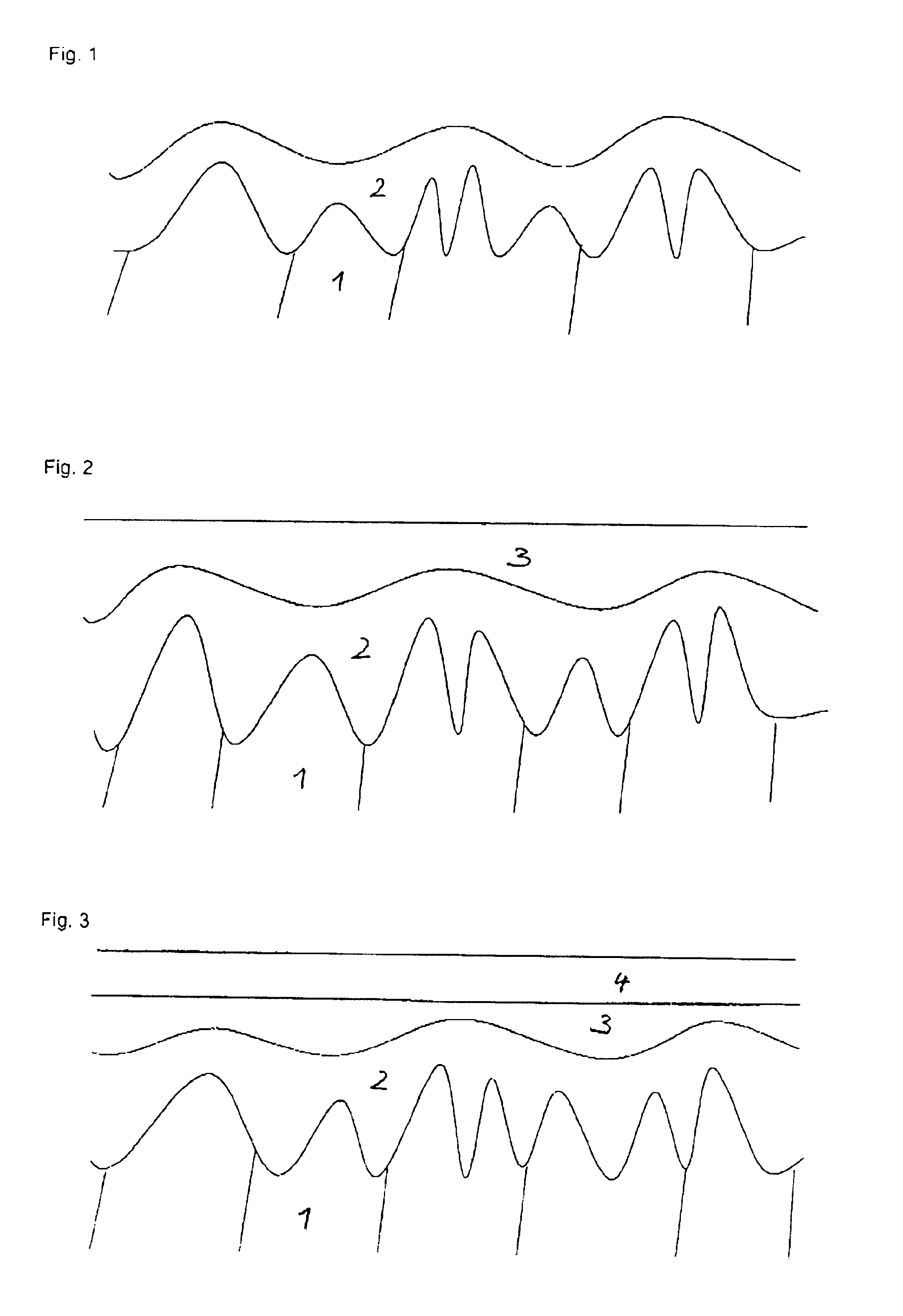

Image

  • Method for the production of optical components with increased stability, components obtained thereby and their use
  • Method for the production of optical components with increased stability, components obtained thereby and their use

Examples


example

A crystal lens of CaF2 material obtained from a homogeneous single crystal by sawing and grinding is polished to micro-roughness. Then it is carefully cleaned in order to remove contamination particles and water components on the surface. Another cleaning step is produced in an evaporation device by glow discharge at room temperature in a time period of approximately 30 minutes. In this way, the temperature of the component increases somewhat. Then a covering layer of SiO2 is deposited in a thickness of 0.5μ. After deposition, the covering layer is processed by polishing to a water-free state with diamond polishing means. Since the surface now no longer has a direction-dependent hardness in the crystal structure, the triple-wave character that is otherwise common in CaF2 remains clearly smaller. Subsequent processes, such as ion-beam abrasion or robotic polishing, permit a further targeted rapid convergence for improving the fit, since the abrasion process is produced here on an alm...


PUM

PropertyMeasurementUnit
thicknessaaaaaaaaaa
thicknessaaaaaaaaaa
thicknessaaaaaaaaaa

Abstract

A method is described for the production of optical components, particularly of crystalline base material, with elevated stability and an optically active three-dimensional shape, which is defined by its surfaces, of high fit accuracy, by shaping the base material into a blank with a desired three-dimensional shape, and applying a covering layer to the surface of the thus-formed three-dimensional shape and the fit accuracy is obtained by abrasion of the covering layer.

Description

BACKGROUND OF THE INVENTIONThe invention concerns a method for the production of optical components, particularly those of a crystalline base material, with an increased stability as well as the components obtained thereby and their use.Optical components, such as lenses and prisms, have been known for a long time for the production of different optics for multiple purposes of application. They are usually comprised of a base material that transmits electromagnetic radiation, and this material has an optically active three-dimensional shape or geometry, which deflects the direction of the wave beam that passes through it at its surfaces when it enters and exits. It usually happens that—insofar as possible—the optically active shape is cast directly in a pattern predominantly in the case of plastics, or in the case of optical glass or crystals is cut out of a block of material by chipping, sawing and grinding.The surface of such optical elements, however, is not completely flat, but ...

Claims


Application Information

Patent Timeline
Patent Type & Authority Patents(United States)
IPC IPC(8): B23K26/40B23K26/00C03C17/23C03C17/34C03C17/22G02B1/00G02B1/02G02B1/10G03F1/08G02B1/11G02B1/111G02B3/00H01L21/027
CPCC03C17/22C03C17/23C03C17/3411G02B1/10G02B1/02C03C2217/213C03C2217/77C03C2218/328C03C2217/285G02B1/11G02B1/14
Inventor SCHUSTER, KARL-HEINZ
Owner CARL ZEISS SMT GMBH
Why Eureka
Eureka Blog
Learn More