Method of manufacturing semiconductor device having trench isolation

a manufacturing method and trench isolation technology, applied in semiconductor devices, semiconductor/solid-state device testing/measurement, electrical equipment, etc., can solve the problems of deterioration in operation breakdown voltage, kinks, and heat treatment after implanting impurities, so as to facilitate analysis on the measurement result of spectroscopic ellipsometry, the effect of suppressing the final depth of trench tr2 and increasing the selectivity of etching on nitride film 22

Inactive Publication Date: 2005-01-11
RENESAS ELECTRONICS CORP
View PDF8 Cites 13 Cited by
  • Summary
  • Abstract
  • Description
  • Claims
  • Application Information

AI Technical Summary

Benefits of technology

An object of the present invention is to provide a method of manufacturing a semiconductor device in which deterioration in a transistor characteristic is avoided by preventing a channel stop implantation layer from being formed in an active region.
After forming the trench for the trench isolation oxide film, the latest etching rate for the SOI layer is calculated, and data of the latest etching rate is given to the trench etching step for a different manufacturing lot of a semiconductor device, so that variations among lots, in the final depth of the trench can be suppressed.
When a combined isolation oxide film is included as the trench isolation oxide film and a portion around the active region except for a portion near a gate electrode of the MOS transistor is constructed by the full isolation oxide film and the other portion is constructed by the partial isolation oxide film, full isolation data for forming a full trench for forming a full isolation oxide film can be easily obtained.

Problems solved by technology

Consequently, there is a tendency that heat treatment after implanting impurities is performed at low temperature in short time.
However, there are various problems caused by a substrate floating effect, such as accumulation of carriers (holes in the NMOS transistor) generated by an impact ionization phenomenon in the channel forming region, occurrence of a kink due to the accumulated carriers, deterioration in operation breakdown voltage, and occurrence of frequency dependency of delay time caused by an unstable potential of the channel forming region.
However, there is a case that, in the well region under the partial isolation oxide film, the impurity concentration decreases due to a segration phenomenon at the time of forming an oxide film, and the conduction type reverses.
Consequently, even if the channel stop implantation is performed before the trench isolation structure is formed, there is the possibility that the impurities are diffused in the heat treatment performed after that, the profile is disturbed, and an intended effect cannot be obtained.
However, in this case, a problem arises such that it is difficult to implant impurities of high concentration into only the region under the trench isolation oxide film.
As a result, it becomes difficult to adjust the threshold value of a MOS transistor and to make the source / drain layer of the MOS transistor or a depletion layer formed around a PN junction of the source / drain layer reach buried oxide film 102.

Method used


Image

  • Method of manufacturing semiconductor device having trench isolation
  • Method of manufacturing semiconductor device having trench isolation
  • Method of manufacturing semiconductor device having trench isolation

Examples


first embodiment

A. First Embodiment

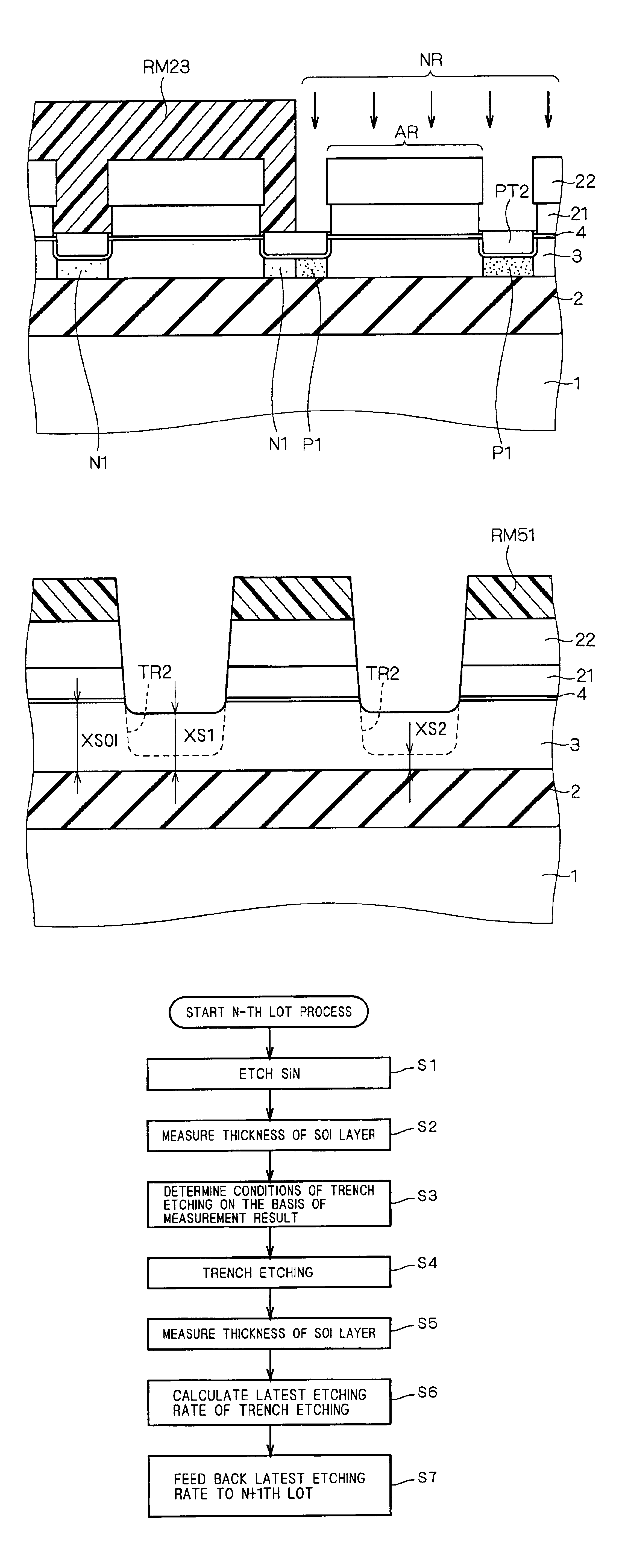
With reference to FIGS. 1 to 13 as cross sections for sequentially showing a manufacturing process, a semiconductor device manufacturing method which prevents a channel stop implantation layer from being formed in an active region will be described.

First, as shown in FIG. 1, by the SIMOX method for forming a buried oxide film 2 (buried insulating film) by oxygen ion implantation, bonding, or the like, an SOI substrate constructed by a silicon substrate 1, buried oxide film 2, and an SOI layer 3 is prepared. The SOI substrate may be formed by a method other than the above methods.

Usually, the film thickness of SOI layer 3 is 50 to 200 nm, and the film thickness of buried oxide film 2 is 100 to 500 nm. On the SOI substrate, a silicon oxide film (hereinafter, called an oxide film) 4 having a thickness of 10 to 30 nm (100 to 300 Å) is formed by CVD (with a temperature condition of about 800° C.) or thermal oxidation (with a temperature condition of 800 to 1000° C.).

Af...

second embodiment

B. Second Embodiment

B-1. Basic Configuration

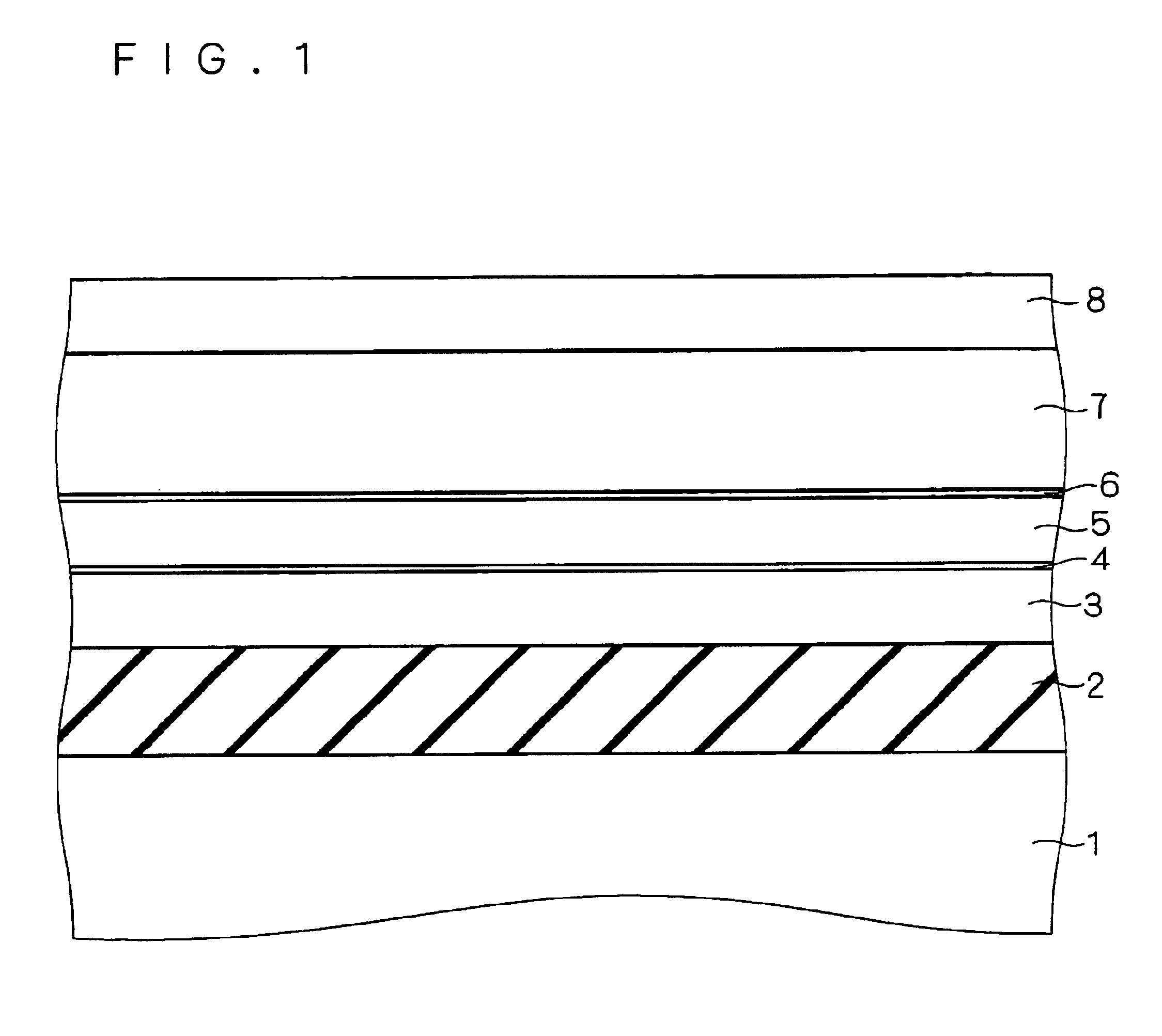
The semiconductor device manufacturing method which prevents the channel stop implantation layer from being formed in an active region described by referring to FIGS. 14 to 20 has the process of forming internal-wall oxide film OX1 by oxidizing the internal wall of trench TR2 prior to filling of trench TR2 with an HDP oxide film as described by referring to FIG. 16. It is more preferable to use dry oxidation performed by furnace anneal in oxygen (O2) atmosphere of 800 to 1000° C. for the oxidizing process.

FIG. 27 shows a sectional shape of internal-wall oxide film OX1 formed by dry oxidation. When dry oxidation is performed as shown in FIG. 27, the thickness of internal-wall oxide film OX1 is not uniform in portions.

Specifically, when the thickness of a portion formed on a side wall of trench TR2 of internal-wall oxide film OX1 is J1, the thickness of a portion formed at the corner on the bottom side of trench TR2 is J2, and the thickness ...

modification 1

B-3. Modification 1

The sectional shape of trench TR2 shown in FIG. 27 is not a rectangular shape but the corner of the bottom is inclined so as to extend toward the opening. This is due to slow progress of etching in the corner portion at the time of performing etching to form the trench.

In such a structure, the width of the isolation defined by the width of the bottom face of the trench is narrowed, and insulation for isolation deteriorates. It is not desirable for trench isolation.

Consequently, at the time of performing etching to form the trench, etching conditions are set to perform rather over-etching, thereby forming a trench TR21 having a mesa sectional shape as shown in FIG. 28.

The side walls of trench TR21 are inclined so that the opening is widened from the nitride film 22 side toward the bottom, and the inclination angle is about 95° to 110°. FIG. 29 shows a state where internal-wall oxide film OX1 by, for example, dry oxidation in trench TR21 having such a shape.

As shown...


PUM


Abstract

The invention relates to improvements in a method of manufacturing a semiconductor device in which deterioration in a transistor characteristic is avoided by preventing a channel stop implantation layer from being formed in an active region. After patterning a nitride film (22), the thickness of an SOI layer 3 is measured (S2) and, by using the result of measurement, etching conditions (etching time and the like) for SOI layer 3 are determined (S3). To measure the thickness of SOI layer 3, it is sufficient to use spectroscopic ellipsometry which irradiates the surface of a substance with linearly polarized light and observes elliptically polarized light reflected by the surface of a substance. The etching condition determined is used and a trench TR2 is formed by using patterned nitride film 22 as an etching mask (S4).

Description

BACKGROUND OF THE INVENTION1. Field of the InventionThe present invention relates to a semiconductor device and, more particularly, to a method of manufacturing a semiconductor device having a trench isolation oxide film.2. Description of the Background ArtA semiconductor device of an SOI (Silicon On Insulator) structure (hereinbelow, called an SOI device), formed on an SOI substrate in which a buried oxide film and an SOI layer are formed on a silicon substrate has characteristics such as reduced parasite capacity, high-speed operation, and low power consumption and is used for a portable device and the like.Also for a bulk device directly formed on a silicon substrate, microfabrication technology and high integration technique progress conspicuously, and the speed of development of the bulk device is increasing.In association with a progress of a device technique, the concentration of a channel impurity and that of a source / drain impurity are getting higher and, moreover, a sharp ...

Claims


Application Information

Patent Timeline
Patent Type & Authority Patents(United States)
IPC IPC(8): H01L21/762H01L29/66H01L29/786H01L21/70H01L21/336H01L27/12H01L21/02H01L21/84H01L21/8244H01L21/66H01L21/76H01L21/8238H01L27/08H01L27/092H01L27/10H01L27/11
CPCH01L21/76264H01L21/84H01L29/78612H01L27/1203H01L29/66772H01L29/78609H01L27/11H01L21/76283H10B10/00H01L21/762
Inventor MATSUMOTO, TAKUJITSUJIUCHI, MIKIOIWAMATSU, TOSHIAKIMAEDA, SHIGENOBUHIRANO, YUUICHIMAEGAWA, SHIGETO
Owner RENESAS ELECTRONICS CORP
Why Eureka
Try Eureka