
Mono-, oligo-and polyalkylidenefluorenes and their use as charge transport materials

a charge transport material and polyalkylthiophene technology, applied in the direction of discharge tube/lamp details, natural mineral layered products, synthetic resin layered products, etc., can solve the problems of reduced device performance, low ionisation potential of poly(3-alkylthiophenes), and high processing cost of vacuum deposition

Inactive Publication Date: 2004-10-19
MERCK PATENT GMBH
View PDF14 Cites 23 Cited by
  • Summary
  • Abstract
  • Description
  • Claims
  • Application Information

AI Technical Summary

Benefits of technology

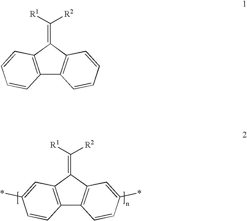
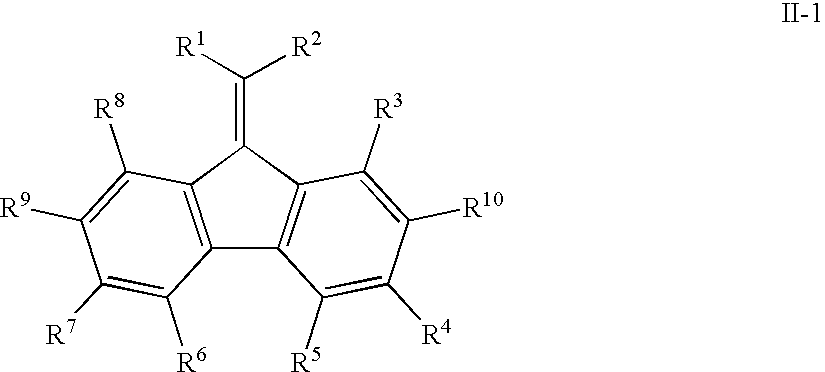
The invention relates to new compounds called mono, oligo, and polymers of 9-alkylidenefluorene. These compounds have potential use as semiconductors or charge transport materials in electronic devices. They have high charge carrier mobility, good processibility, and improved oxidative stability. The invention also provides methods for preparing these compounds. The technical effects of the invention are improved performance and lower cost of organic based thin film transistors and organic field effect transistors.

Problems solved by technology

In addition, it is important that the semiconducting material is relatively stable to oxidation, i.e., it has a high ionisation potential, as oxidation leads to reduced device performance.
However, vacuum deposition is an expensive processing technique that is unsuitable for the fabrication of large-area films.
However, poly(3-alkylthiophenes) have relatively low ionisation potentials and are susceptible to doping in air [see H. Sirringhaus et al., Adv.
These two methods are not readily amenable to the preparation of molecules with alkyl chains larger than propyl.
Moreover, polymers of unsymmetrical 9-alkylidenefluorenes have the general problem of poor regioregularity and therefore poor ordering and packing in the solid state.
This stacking allows intermolecular charge transport to occur more easily, leading to high charge carrier mobilities.
If SCLCPs are used in solutions, they can orient spontaneously when coated onto an appropriate surface and when at their mesophase temperature, which can result in large area, highly ordered domains.

Method used


Image

  • Mono-, oligo-and polyalkylidenefluorenes and their use as charge transport materials
  • Mono-, oligo-and polyalkylidenefluorenes and their use as charge transport materials
  • Mono-, oligo-and polyalkylidenefluorenes and their use as charge transport materials

Examples


example 1

2,7-Dibromofluorenone (1) was prepared as described below: ##STR14##

2,7-Dibromofluorene (20.00 g, 61.72 mmol), potassium permanganate (31.61 g, 200.0 mmol) and copper(II) sulphate pentahydrate (49.94 g, 200.0 mmol) were ground together to afford a fine powder. The powder was heated at 175-180.degree. C. for 6 h. After cooling to room temperature, tetrahydrofuran (1 L) was added and the mixture was sonicated for 30 minutes before being filtered through celite. The solvent was removed under reduced pressure to afford a crude product, which was triturated with hot methanol (300 mL) and filtered before being dried under reduced pressure to afford 2,7-dibromofluorenone (1) (17.94 g, 86%) as a yellow solid, purity 100% (GC): .sup.1 H and 13C NMR spectra as expected; M.sup.+ =338 (t).

2,7-Dibromo-9-dibromomethylenefluorene (2) was prepared as described below: ##STR15##

Triphenylphosphine (34.89 g, 133.0 mmol) was added to a solution of 2,7-dibromofluorenone (17.94 g, 53.08 mmol) in anhydrous...

example 2

2,7-Dibromo-9-(bis-pentylsulfanyl-methylene)fluorene (4) was prepared by a procedure as described in example 1 (63%): ##STR17##

.delta..sub.H (CDCl.sub.3, 300 MHz) 9.1 (2H, s), 7.50 (2H, d), 7.40 (2H, d), 3.05 (4H) 1.65 (4H, m), 1.5-1.3 (8H, m), 0.85 (6H, t); .delta..sub.c (CDCl.sub.3, 75 MHz) 145.4, 139.7, 137.5, 136.1, 130.28 (ArCH), 129.4 (ArCH), 121.0, 120.3 (ArCH), 36.3, 31.0, 29.8, 22.3, 14.0; M.sup.+ =540 (t).

example 3

2-Bromo-9-(bis-methylsulfanyl-methylene)fluorene (5) was prepared as described in example 2 using methyliodide as the alkylating agent. (76%). M.sup.+ =350 (d). .sup.1 H NMR displayed the expected signals. ##STR18##


PUM

PropertyMeasurementUnit
carrier mobilitiesaaaaaaaaaa
temperatureaaaaaaaaaa
charge transport propertiesaaaaaaaaaa

Abstract

Conjugated mono-, oligo- and polyalkylidenefluorenes are suitable for use as semiconductors or charge transport materials in optical, electrooptical or electronic devices including field effect transistors, electroluminescent, photovoltaic and sensor devices.

Description

The invention relates to new conjugated mono-, oligo- and polyalkylidenefluorenes. The invention further relates to methods for their preparation, their use as semiconductors or charge transport materials in optical, electrooptical or electronic devices including field effect transistors, electroluminescent, photovoltaic and sensor devices. The invention further relates to field effect transistors and semiconducting components comprising the new mono-, oligo- and polymers.BACKGROUND AND PRIOR ARTOrganic materials have recently shown promise as the active layer in organic based thin film transistors and organic field effect transistors [see H. E. Katz, Z. Bao and S. L. Gilat, Acc. Chem. Res., 2001, 34, 5, 359]. Such devices have potential applications in smart cards, security tags and the switching element in flat panel displays. Organic materials are envisaged to have substantial cost advantages over their silicon analogues if they can be deposited from solution, as this enables a f...

Claims


Application Information

Patent Timeline
Patent Type & Authority Patents(United States)
IPC IPC(8): C07C323/07C07C323/00C08G61/00C08G61/02C09K19/38C09K19/32H01L51/05H01L51/30H01L51/50C07C321/20C07C323/06H01B1/12H01L29/786
CPCC07C323/07C08G61/02C09K19/32C09K19/3804H01L51/0039C09K19/3833C07C2103/18Y10T428/10H01L51/0508H01L51/5012Y10S428/917Y02E10/549C07C2603/18Y10T428/3154C09K2323/00H10K85/115H10K10/46H10K50/11C07C321/20
Inventor HEENEY, MARTINTIERNEY, STEVENGILES, MARKFARRAND, LOUISE DIANESHKUNOV, MAXIMSPARROWE, DAVIDMCCULLOCH, IAIN
Owner MERCK PATENT GMBH
Learn More