
Method of preparing for structural analysis a deep trench-type capacitor and method of structural analysis therefor

a technology of capacitors and structural analysis, applied in the direction of individual semiconductor device testing, semiconductor/solid-state device testing/measurement, instruments, etc., can solve the problems of capacitor holes, capacitor holes, metal shorts, and different types of structural defects that can occur during semiconductor fabrication,

Inactive Publication Date: 2002-06-11
PROMOS TECH INC
View PDF5 Cites 11 Cited by
  • Summary
  • Abstract
  • Description
  • Claims
  • Application Information

AI Technical Summary

Benefits of technology

More specifically, the present invention is directed to a method of preparing for structural analysis a deep trench-type capacitor formed in a semiconductor die, employing a combination of mechanical and chemical action to expose the trench-type capacitors. The method of preparing the die includes the steps of (a) mechanically treating the substrate disposed at the die back side so as to remove a first portion of the substrate and leave intact a second portion of the substrate; (b) mounting the mechanically treated die by affixing the die by its top side to a mount; and (c) chemically treating the die so as to remove the substrate second portion. By exposing the deep trench capacitors, the method facilitates the inspection of the device for the detection of possible structural defects such as metal shorts, capacitor holes, and particle failures. The method further overcomes the deficiencies associated with conventional methods of substrate removal, and facilitates inspection by a variety of methods. The method facilitates, for example, the detection of residual arsenic glass, and deep trench deformities, such as those associated with deep trench length and the thickness of the deep trench ON layer.
The present invention, therefore, provides a method of preparation which advantageously overcomes the deficiencies associated with conventional methods, and which is advantageously suitable for any service in which a simple and fast method of preparation is desired. The method facilitates, for example, the detection of residual arsenic glass, and deep trench deformities, such as those associated with deep trench length and the thickness of the deep trench ON layer.
Also, compared to the above-discussed technique of U.S. Pat. No. 5,064,498, the mechanical treatment to remove the first portion of the substrate according to the present invention facilitates more precise control of the thickness of the removed portion of the substrate and is quicker. Further, while the reaction of a choline / water solution is slow and unstable, with difficult determination of the stop point, the RON solution employed in the present invention is a common and safe solution.

Problems solved by technology

For various reasons, different types of structural defects can occur during fabrication of the semiconductor.
These include such defects as metal shorts, capacitor holes, particle failures, incomplete deep trench formation and deformation.
Because the semiconductors have become so miniaturized, however, the ability to detect such structural defects has become more challenging.
However, in this prior art process, it is difficult to control the chemical etching of the substrate to remove a precise thickness thereof; thus, the risk of removing the deep trench capacitor is great.
Also, the chemical etching requires a long time to effect.
Further, the reaction of the choline / water solution is slow and unstable, and it is difficult to determine the stop point.

Method used


Image

  • Method of preparing for structural analysis a deep trench-type capacitor and method of structural analysis therefor
  • Method of preparing for structural analysis a deep trench-type capacitor and method of structural analysis therefor
  • Method of preparing for structural analysis a deep trench-type capacitor and method of structural analysis therefor

Examples


Embodiment Construction

The present invention will be described in terms of the currently perceived preferred aspects thereof.

The present invention is directed to a method of preparing for structural analysis a deep trench-type capacitor, and a method of structural analysis therefor.

In a first aspect of the invention, therefore, the invention relates to a method of preparing for structural analysis a deep trench-type capacitor formed in a die.

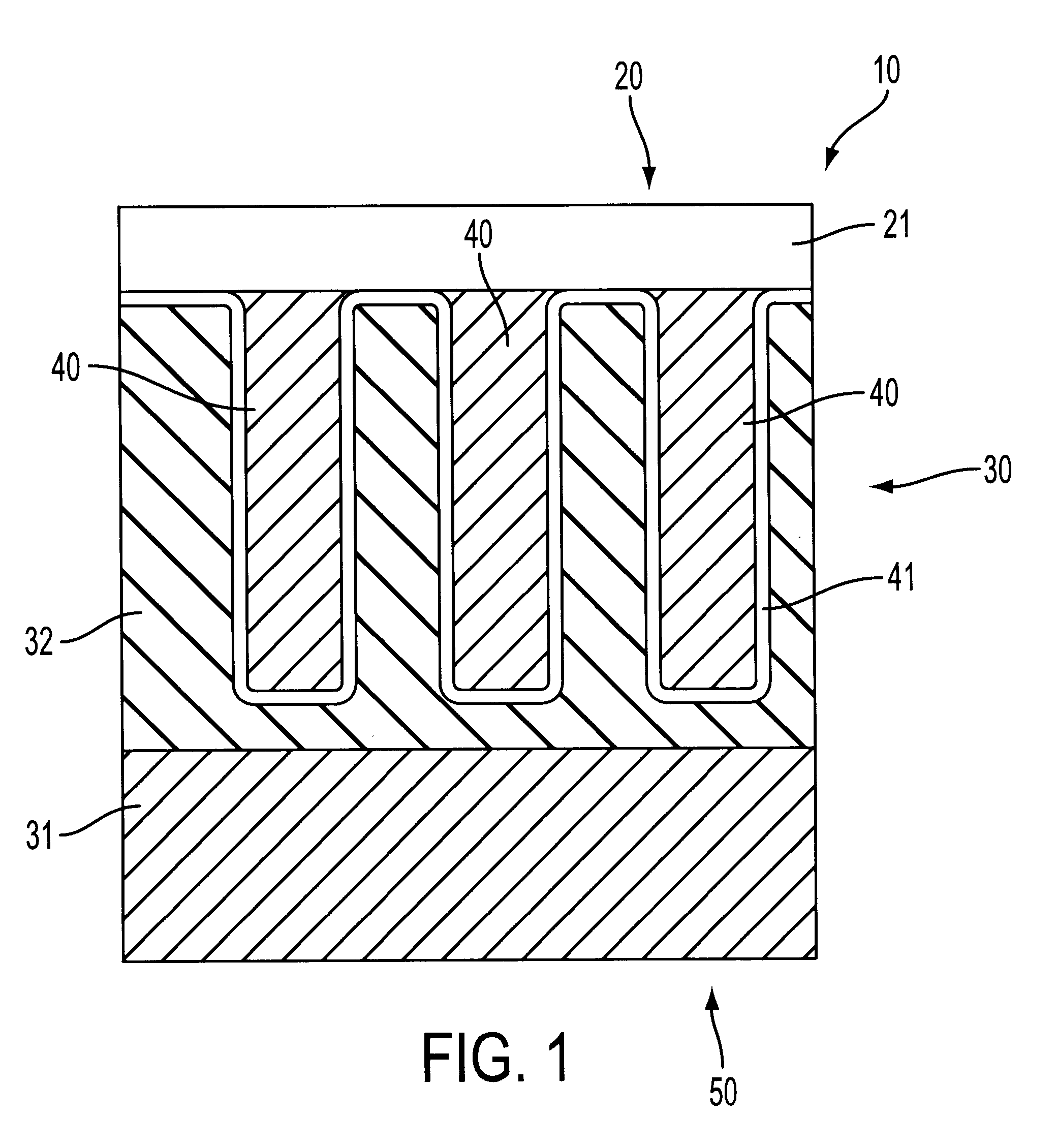
Referring to FIG. 1, the die 10 comprises in general a die top side 20, a substrate 30, a plurality of deep trench capacitors 40 disposed in substrate 30, and a die back side 50. Reference numeral 41 denotes a dielectric of, for example, nitride / oxide, and reference numeral 21 denotes the top portion of the die including for example bit line, word lines, oxide layers, etc.

The method of preparing for structural analysis a deep trench-type capacitor formed on a die 10 comprises the steps of (a) mechanically treating the die back side 50 so as to remove the substrate fir...


PUM


Abstract

A method of preparing for structural analysis a deep trench-type capacitor formed in a die employs a combination of mechanical and chemical action to expose the trench-type capacitors. The method of preparing the die includes the steps of (a) mechanically treating the die back side so as to remove a first portion of the substrate and leave intact a second portion of the substrate; (b) mounting the mechanically treated die by affixing the die by its top side to a mount; and (c) chemically treating the mounted die so as to remove the substrate second portion and provide a chemically treated die. By exposing the deep trench capacitors, the method facilitates the inspection of the device for the detection of possible structural defects such as metal shorts, capacitor holes, and particle failures. The method further overcomes the deficiencies associated with conventional methods of substrate removal, and facilitates inspection by a variety of methods. The method facilitates, for example, the detection of residual arsenic glass, and deep trench deformities, such as those associated with deep trench length and the thickness of the deep trench ON layer.

Description

1. Field of the InventionThis invention relates generally to a method of preparing for structural analysis a deep trench (DT)-type capacitor, and a method of structural analysis therefor. The invention relates more specifically to a method of preparation which employs a combination of mechanical and chemical action to expose the trench-type capacitors for structural analysis.2. Description of Related ArtDemands for miniaturization in the semiconductor industry require that a higher density of electronic devices such as capacitors be placed on a chip.One solution to the demand for higher density capacitors is the use of trench-type capacitors. In a trench-type capacitor, advantage is taken of the depth of the substrate in order to place a high density pattern of capacitors on the semiconductor device. For example, U.S. Pat. No. 6,071,823 describes a method of fabricating a bottle-shaped deep trench in a semiconductor substrate.For various reasons, different types of structural defect...

Claims


Application Information

Patent Timeline
IPC IPC(8): H01L21/02H01L21/70H01L21/334H01L21/8242H01L27/08
CPCH01L27/0805H01L29/66181H01L27/10861H10B12/038
Inventor LEE, THING-JONG
Owner PROMOS TECH INC
Learn More