
Memory redundancy device and method

a memory redundancy and circuit technology, applied in the field of redundancy circuitry for semiconductor memory devices, can solve the problems of significant reduction of achieve the effects of reducing the processing yield of large-scale memory arrays, improving the processing yield of memory chips, and reducing chip manufacturing costs

Inactive Publication Date: 2001-06-05
STMICROELECTRONICS SRL
View PDF8 Cites 10 Cited by
  • Summary
  • Abstract
  • Description
  • Claims
  • Application Information

AI Technical Summary

Benefits of technology

Processing defects in static random access memory (SRAM) and dynamic random access memory (DRAM) devices can significantly reduce the processing yield in large scale memory arrays. In order to improve the processing yield of memory chips, various methods of error correction have been created. These include `soft` error correcting whereby software corrects for physical defects, and `hard` error correcting whereby defective circuit elements are replaced with redundant elements included on the chip. The use of soft or hard error correcting can result in lower chip manufacturing costs and earlier introduction of new products on existing wafer fabrication lines or in new process technologies.
Yield enhancement by `hard` error correcting on a memory chip is typically produced by including redundant rows and / or columns within the memory array. A few redundant rows or columns can significantly enhance yield of a memory circuit since many devices are rejected for single bit failure or failures in a single row or column. These redundant rows or columns can be added to the memory design to replace defective rows or columns which are identified at electrical test after wafer processing.
According to the present invention, there is provided a redundant circuit and method for a memory device having a plurality of row and column lines, including a programmable circuit for indicating at least one row or column line having a defect and a shifter circuit for shifting the memory addresses to bypass the at least one indicated defective row or column line. In particular, the shifter circuit modifies the address mapping for the row or column lines initially mapped to address values which are greater than the address value corresponding to the defective row or column line indicated by the programmable circuit. For each row or column line initially mapped to an address value which is greater than the address value corresponding to the defective row or column line, the shifter circuit maps a new address value to the row or column line which is one less than the address value initially mapped thereto. The highest numbered address values are mapped to a redundant row or column line. In this way, the defective row or column line is effectively bypassed.
In the first preferred embodiment of the present invention described above, the address value corresponding to a defective row or column line, generated by the programmable circuitry, is static so that an entire column or row line associated with at least one defect is permanently bypassed. In a second preferred embodiment of the present invention, the address value corresponding to a defective column line is dynamically generated in order to bypass the column line only when a previously discovered defective memory cell is to be accessed. In this way, a single redundant column line may be utilized to bypass defective memory cells associated with different column lines.

Problems solved by technology

Processing defects in static random access memory (SRAM) and dynamic random access memory (DRAM) devices can significantly reduce the processing yield in large scale memory arrays.
A problem exists, however, concerning the layout of the fuse elements and the memory array in that the fuse elements are large relative to the dimensions of a memory cell such that the pitch of a fuse element is generally greater than the column or row pitch for memory devices utilizing today's advanced fabrication techniques.

Method used


Image

  • Memory redundancy device and method
  • Memory redundancy device and method
  • Memory redundancy device and method

Examples


Embodiment Construction

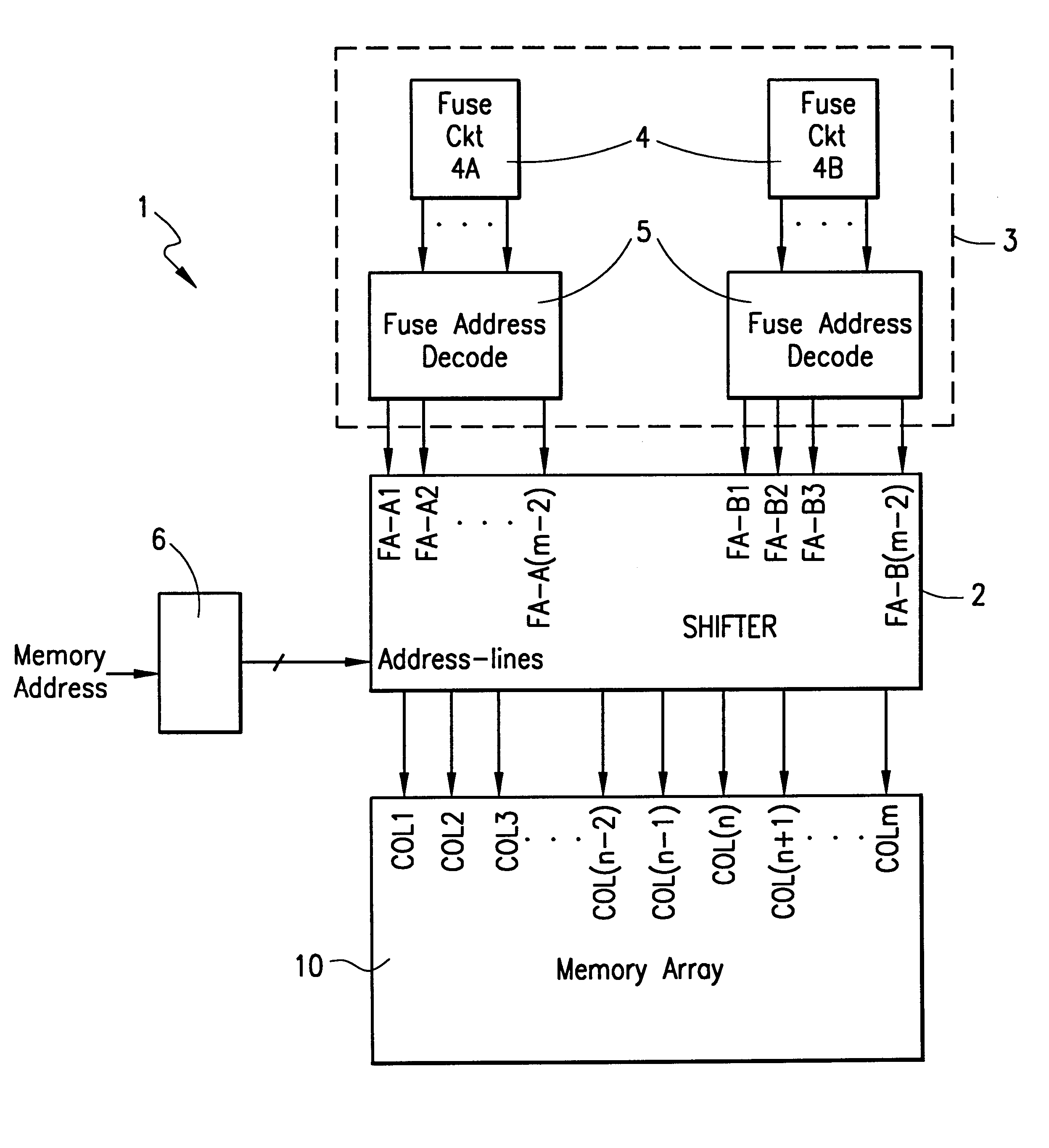
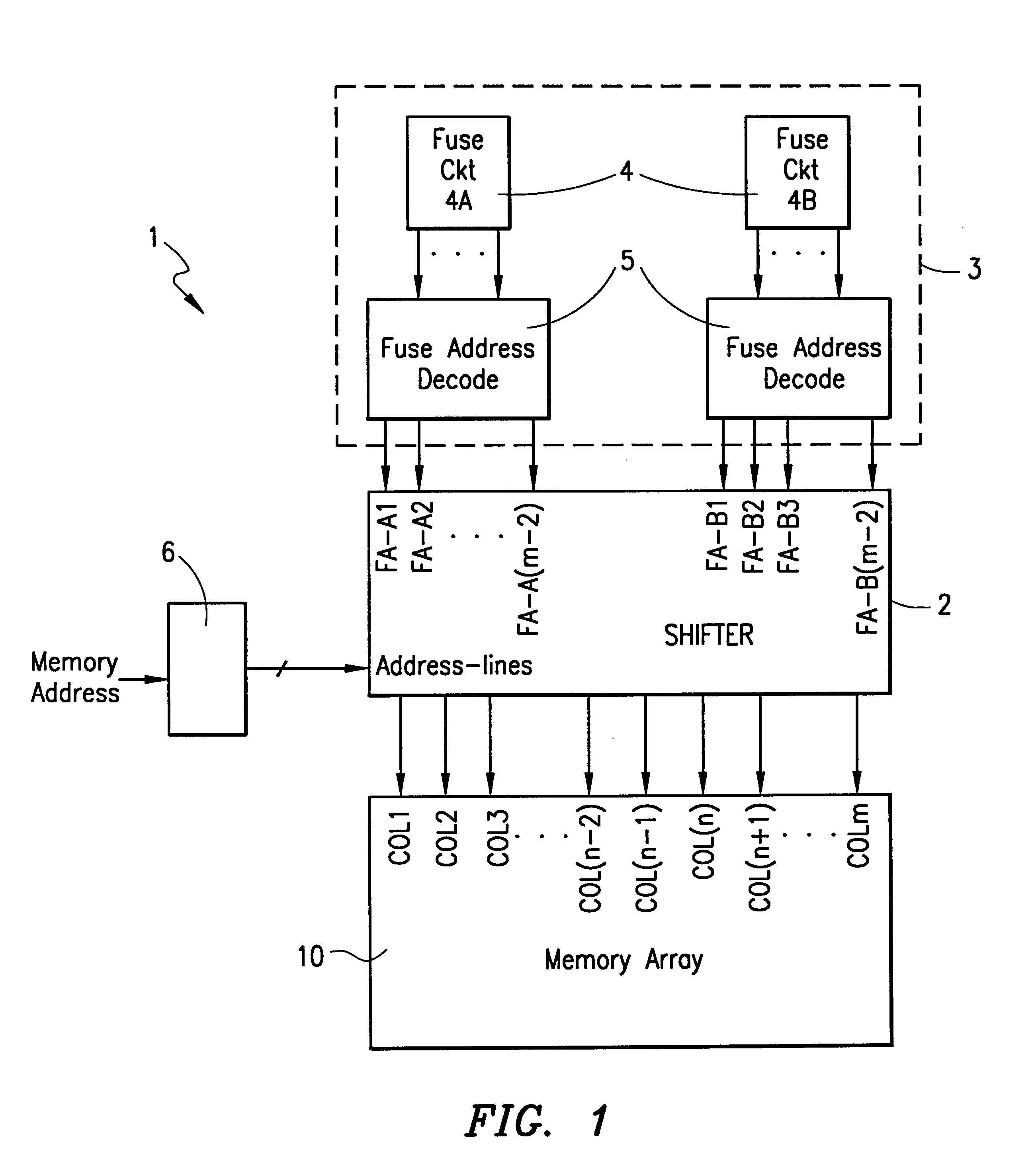
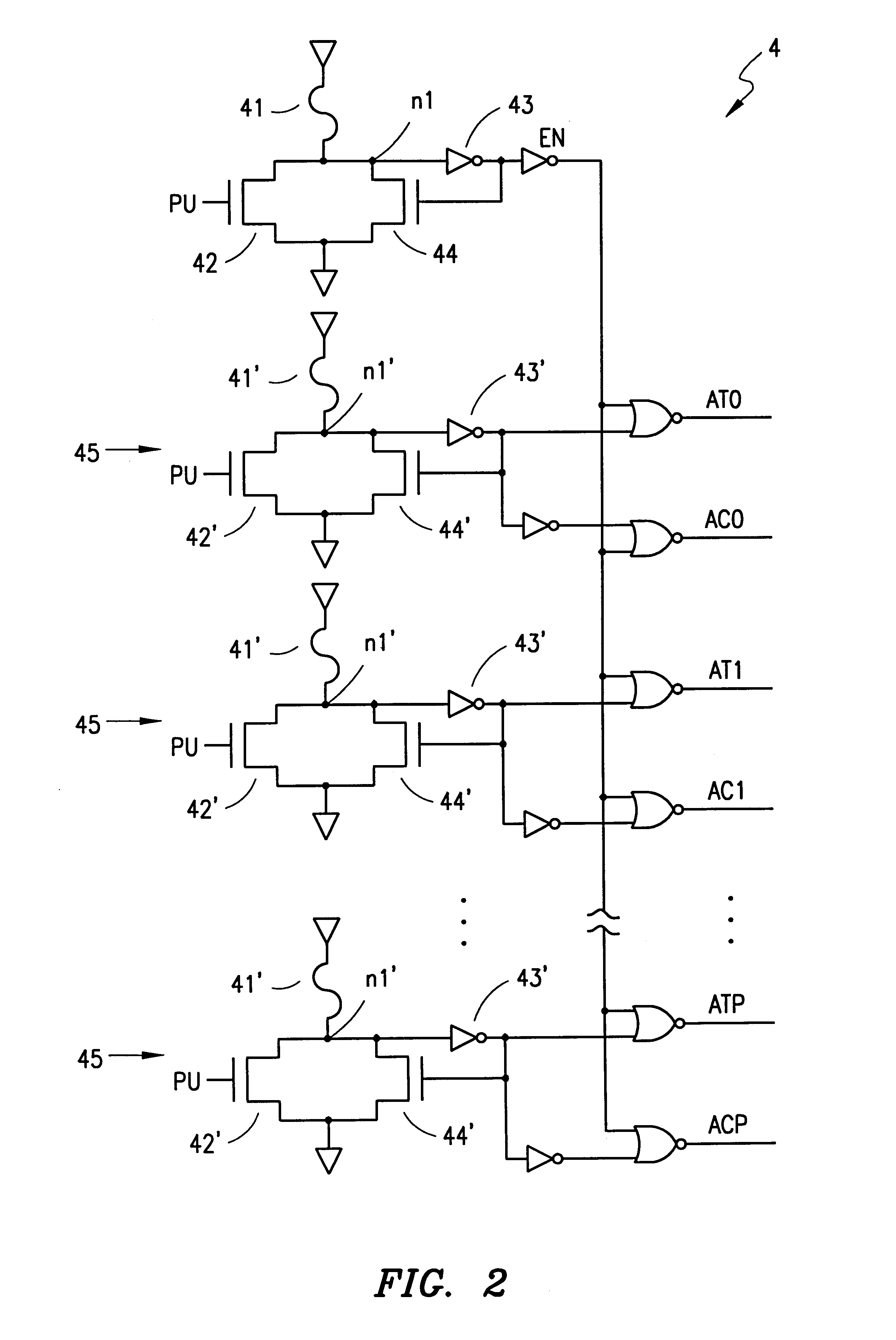
Referring to FIGS. 1-3, there is shown a redundancy circuit 1 which is suitably employed to indicate and effectively bypass row or column lines associated with a defect, such as a manufacturing defect. Redundancy circuitry 1 is adapted to directly drive the row or column lines of a memory array 10. Memory array 10 includes additional (redundant) row or column lines for use upon discovery of a row or column line being associated with a defect. For purposes of simplicity, redundancy circuit 1 will be described below in conjunction with the column lines of memory array 10. It is understood that the present invention may be suitably employed to effectuate the replacement of defective memory row lines of memory array 10.

Redundancy circuit 1 preferably includes a shifter circuit 2 and a programmable circuit 3. Programmable circuit 3 is selectively programmed to indicate one or more previously discovered column lines having a defect associated therewith. Shifter circuit 2 controls the acti...


PUM


Abstract

A redundant circuit and method for a semiconductor memory device is disclosed. The redundant circuit includes a programmable circuit for selectively generating at least one first address corresponding to a defective memory row or column line, and shifter circuitry for remapping second addresses which are greater than the first address to row / column lines. For each second address which is greater than the first address, the shifter circuitry remaps the second address to a row / column line which was initially mapped to an immediately higher address relative to the second address. The programmable circuit is capable of generating a plurality of first addresses corresponding to a plurality of defective memory row or column lines.

Description

1. Technical Field of the InventionThe present invention relates to redundancy circuitry for semiconductor memory devices, and particularly to row / column redundancy circuitry for random access memory (RAM) devices.2. Background and Objects of the InventionProcessing defects in static random access memory (SRAM) and dynamic random access memory (DRAM) devices can significantly reduce the processing yield in large scale memory arrays. In order to improve the processing yield of memory chips, various methods of error correction have been created. These include `soft` error correcting whereby software corrects for physical defects, and `hard` error correcting whereby defective circuit elements are replaced with redundant elements included on the chip. The use of soft or hard error correcting can result in lower chip manufacturing costs and earlier introduction of new products on existing wafer fabrication lines or in new process technologies.Yield enhancement by `hard` error correcting ...

Claims


Application Information

Patent Timeline
Patent Type & Authority Patents(United States)
IPC IPC(8): G11C29/00G11C11/401G11C11/413G11C29/04H01L21/82
CPCG11C29/78
Inventor BRADY, JAMES
Owner STMICROELECTRONICS SRL
Learn More