
Property estimation of an integrated circuit

Inactive Publication Date: 2000-05-23
EDINBURGH UNIV OF
View PDF4 Cites 111 Cited by
  • Summary
  • Abstract
  • Description
  • Claims
  • Application Information

AI Technical Summary

Benefits of technology

Sampling also permits analysis of modifications to the integrated circuit design itself, for example, layout modifications such as: the insertion of redundant contacts; track displacements; track width increases etc., used to increase device robustness and enhanced yield. An estimate of the possible number or amount of such modifications can be made. The consequences of these layout modifications on devices properties either directly affected or indirectly affected can also be estimated.

Problems solved by technology

Such defects are small randomly occurring particles of foreign matter, of varying size, present in the manufacturing process.
These defects can fatally damage an integrated circuit during manufacture.
It is not uncommon for such an analysis to require hundreds of hours of computer time and a large amount of computer memory.
A substantial cost must be incurred to estimate these properties and other properties of an integrated circuit.
This has the obvious disadvantage that a network of computers must be provided at high cost.
There is also the additional burden of managing the distribution of the calculation over the network, which is typically in use by other users for different applications.
The technique is limited by the nature of the design hierarchy.
However, many integrated circuit devices do not follow this pattern.
This almost always leads to a degree of inaccuracy.
The level of inaccuracy is not easily predicted, and can be large.
Consequently, it is not possible to use the results with confidence.
The implementation is considerably more difficult.
Even exploiting the hierarchy of a design the extraction of device properties can still take a considerable time.
This is a costly solution in that it combines a complex implementation with costly hardware.
Both the complex software and its use within a network, which can be subject to change, must be maintained at substantial cost.
The disadvantage of this approach is that it requires a person skilled in the art to select an appropriate characteristic block or blocks.
A further disadvantage is that results based on this approach can be very variable depending on the skill of the practitioner, the actual layout and characteristic region selected.
It is also difficult to determine how much reliance can be placed on any estimate.
Also, not all integrated circuit designs are suitable for this method since they may be highly variable and not contain blocks that obviously contain similar cells or characteristics.
However, it has a number of limitations.
The most obvious limitation is that a design must be composed using a known and characterized design environment.
Not all design environments will be simple to characterize, particularly where they are not limited to special applications.
The history of the various parts is not always available and so cannot be used to estimate device properties.
The same extractions using a hierarchical implementation that ignores cell interaction had taken many tens of hours.
These hierarchical extractions also required large amounts of memory and as a result used a computer specially configured for memory intensive applications.
A flat extraction was not feasible on such large designs with the available computing resources.
The memory requirements for flat extractions are very large.
Such techniques are not generally considered practical because of the time and / or computer memory requirements.
A mismatch between the representation and the actual device can result in inaccurate property measurements.
Unless precautions are taken, the sizing and other modifications can change the layout within the sample inappropriately, such that it is not properly representative of the integrated circuit after the same operation.
In some cases it is not possible to correctly determine connectivity without analysing the whole layout.
However, some properties are obtained from measurements of polygons that are only valid within a smaller region of the measurement region.
The small hole provides a conduction path between electrically separate nodes, causing a circuit fault.
This implies that a measure of extra material critical area from a measurement region will not accurately reflect the critical area of the same layout in the circuit.
A valid measurement region is used rather than using polygons in the skirt region because the connectivity of geometry in the skirt region cannot be guaranteed.
Some local connections to skirt layout geometry may not be present and hence the connectivity information is not accurate enough.
However this approach cannot be used where polygons have been cut, as estimates based on this count would tend to give over-estimates.
Many integrated circuit technologies, particularly older technologies, do not have design rules which require a fixed contact / via size.
However, where the size of the contacts is unknown this approach would require a measure of the average contact size.
However, the valid measurement region is smaller using this technique.
In general this results in a greater variance and hence larger errors in the estimation.
However, the result is still a good estimate of the complexity of a circuit since the larger transistors are usually associated with buffers rather than logic gates.
However, this may result in inaccurate error bounds since fault mechanisms are normally correlated to some degree.

Method used


Image

  • Property estimation of an integrated circuit
  • Property estimation of an integrated circuit
  • Property estimation of an integrated circuit

Examples


Embodiment Construction

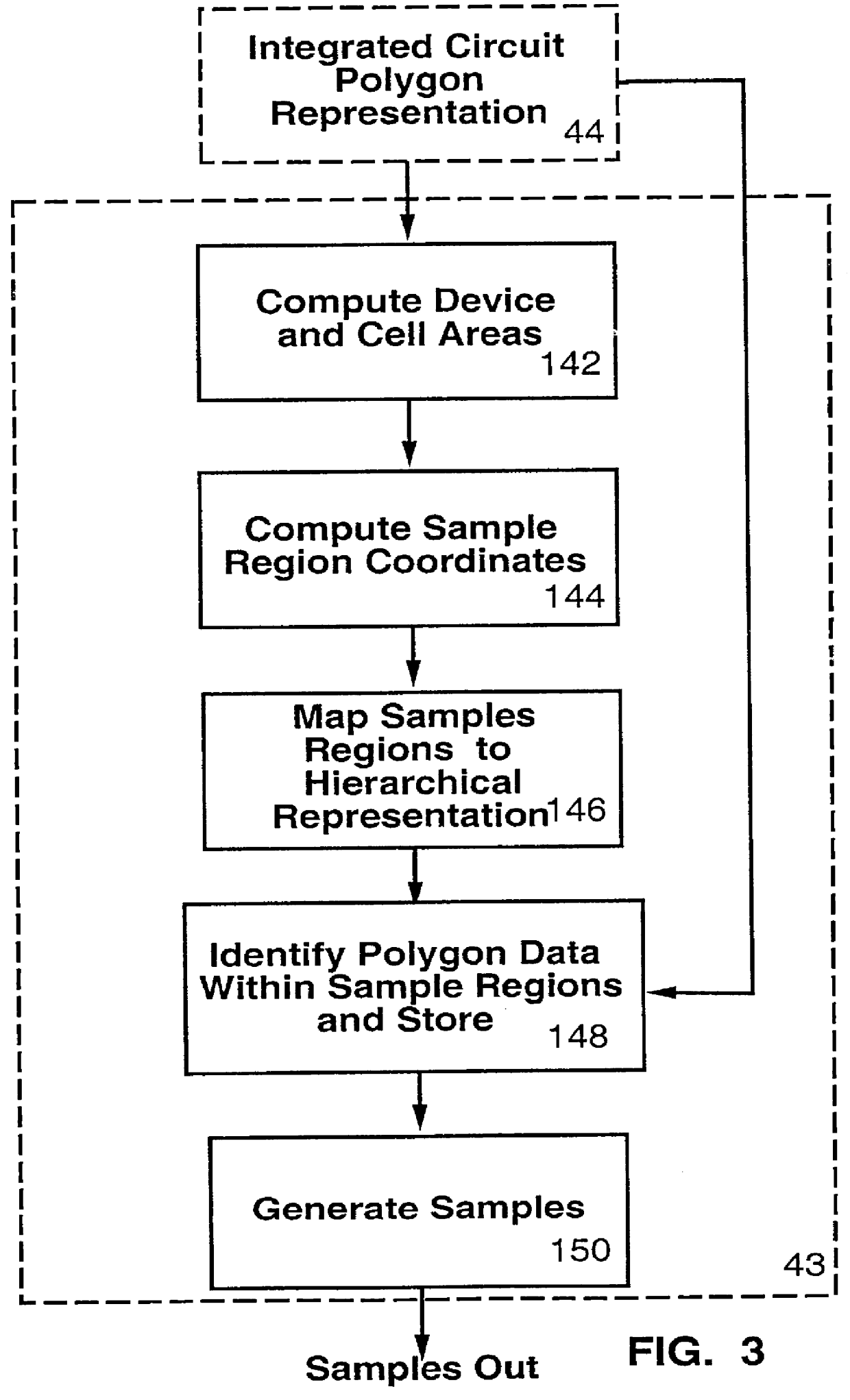
It will be clear, to those skilled in the art, in the light of the teaching presented here that there are other possible embodiments of the invention. In particular, existing tools for geometry manipulation can be used to perform a similar set of operations. These tools are commonly used within the design and fabrication of integrated circuit and often take the form of design rule checkers. A commonly used tool is the Dracula design rule checker produced by Cadence Design Systems, Inc of San Jose. In the preferred embodiment of the present invention samples are taken one at a time from the representation and processed. Using a design rule checker it would be straight forward, for those skilled in the art, to generate a masking layer of sample regions. This masking layer could be used to generate the required samples using a Boolean AND operation or other operators. This would reduce the amount of mask data to only that present within the sample regions. Property estimation of these ...


PUM


Abstract

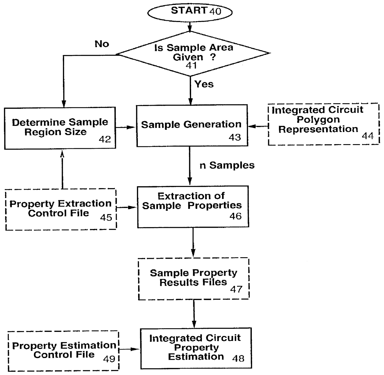
A method and apparatus to estimate properties of an integrated circuit device utilizes reduced resources. The representation of an integrated circuit is sampled using the statistical techniques of survey sampling. An average value of a property is determined from these samples and used to determine the property of the integrated circuit as a whole. Thus a property of an integrated circuit is determined from an analysis of a fraction of the integrated circuit representation. Error bounds associated with the property can be optionally determined from the estimated variance of the sampled property measurements. The method is realized using a general purpose computer. The invention has application to the estimation of integrated circuit manufacturability, yield and other properties.

Description

BACKGROUND TO THE INVENTION1) Field of the InventionThis invention relates to the design and manufacture of integrated circuits and more particularly to a method of estimating properties of an integrated circuit.2) Description of the Background ArtIn the design and manufacture of integrated circuits it is required to estimate particular properties of an integrated circuit. An example of such a property is the sensitivity or susceptibility to extra material defects. Extra material critical area is a measure of an integrated circuit layout geometry that defines the susceptibility of the device to extra material defects of a given size. Such defects are small randomly occurring particles of foreign matter, of varying size, present in the manufacturing process. These defects can fatally damage an integrated circuit during manufacture. It is common practice to extract and compute a value for extra material critical area for a range of discrete defect sizes. These results are combined to ...

Claims


Application Information

Patent Timeline
IPC IPC(8): H01L21/66
CPCH01L22/20H01L2224/48091H01L2924/00014
Inventor ALLAN, GERARD ANTHONY
Owner EDINBURGH UNIV OF
Learn More