
Laser repair process for printed wiring boards

a laser repair and printed wiring technology, applied in the direction of printed circuit repair/correction, manufacturing tools, removing conductive materials by irradiation, etc., can solve the problems of affecting affecting the quality of printed circuit boards, and corresponding increase in pc board costs. achieve the effect of improving the yield of densely wired pc boards

Inactive Publication Date: 2000-04-04
IBM CORP
View PDF16 Cites 24 Cited by
  • Summary
  • Abstract
  • Description
  • Claims
  • Application Information

AI Technical Summary

Benefits of technology

It is therefore a purpose of the present invention to improve densely wired PC board yield;
It is another purpose of the present invention to reduce the cost of densely wired PC boards;
It is yet another purpose of the present invention to simplify wiring short removal on densely wired PC boards.
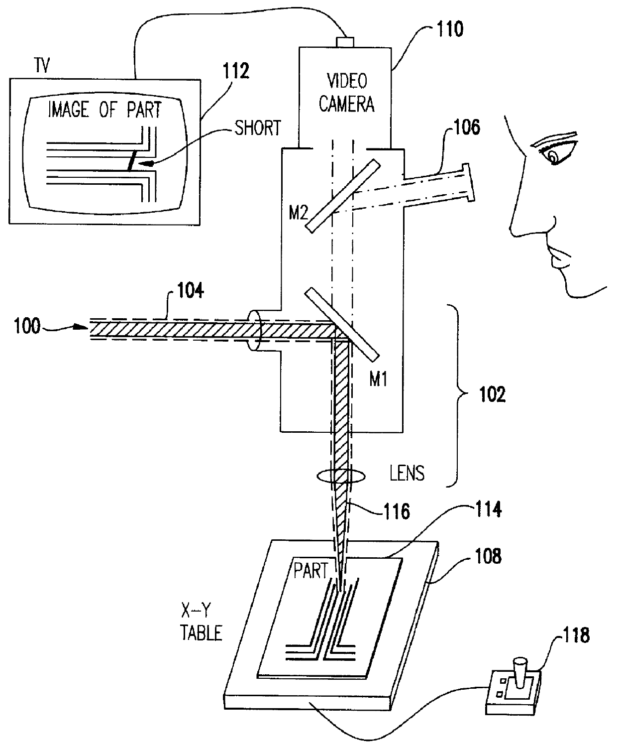
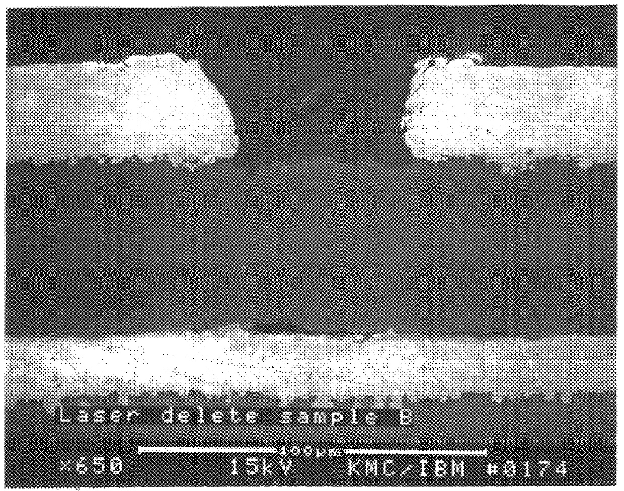
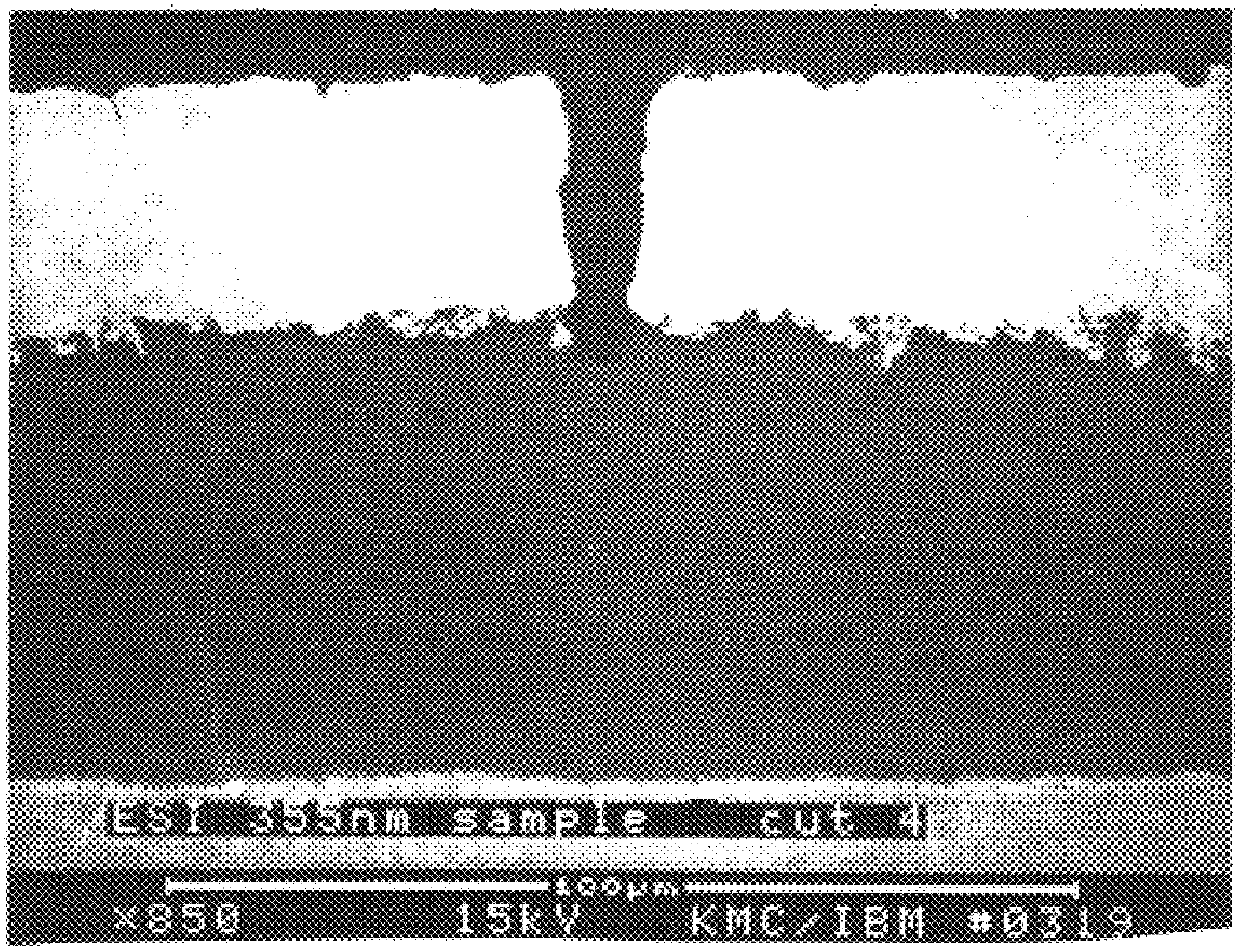
The present invention is method of selectively trimming metal from a surface layer of an insulator material without damaging wiring buried in or beneath the material. A laser is selected with a wavelength such that it is partially absorbed between 1-10% by the dielectric material. Preferably, it is absorbed between 2-5%. Thus, when the metal is ablated or etched from the dielectric surface, etching continues slightly into the surface. However, the laser is prevented from completely etching through or passing through the dielectric, and inadvertently ablating metal therein or thereunder.

Problems solved by technology

One result of increasing wiring density is a corresponding increase in PC board costs.
Excimer lasers, which are expensive and difficult to maintain, are normally used to repair surface wiring on ceramic substrates.
However, a typical excimer laser used to repair a short on a ceramic surface would pass through an organic surface layer of an SLC board, damaging underlying wiring.
Also, Xenon lasers with a wavelength in the blue-green range (450-570 nm) have been found to pass through an organic surface layer, damaging any underlying wires.
Thus, these types of lasers may not be used to repair defects (especially shorts) in dense SLC surface wiring.
Unfortunately, cutting the short may also damage the PC board being repaired.
The knife may slip and damage the SLC.
Further, as wiring density increases, cutting becomes very difficult.
So, for dense wiring on an organic insulator, such as an SLC, manual repair is inconsistent at best.

Method used


Image

  • Laser repair process for printed wiring boards
  • Laser repair process for printed wiring boards
  • Laser repair process for printed wiring boards

Examples


Embodiment Construction

A dielectric known as Advanced Solder Mask (ASM) is a photosensitive dielectric material that may be patterned directly to form through-holes, known as vias, that connect wiring layers at opposite surfaces of an ASM layer. ASM material is described in U.S. Pat. No. 5,026,624 entitled "Composition for Photo Imaging" to Day et al., and in U.S. Pat. No. 5,300,402 entitled "Composition for Photo Imaging" to Card et al., both assigned to the assignee of the present invention and incorporated herein by reference. Surface Laminar Circuit (SLC) boards made from ASM (SLC / ASM) exhibit a dramatic increase in wiring density over other SLCs, because very small vias may be formed with very high precision.

The inventor has discovered that laser ablation may be used to successfully repair or modify copper wiring formed on an SLC / ASM surface by selecting a laser that is slightly absorbed (1-10%) by the ASM material. Thus, the ASM material is neither reflective, transparent, nor fully absorbing, but m...


PUM

PropertyMeasurementUnit
Fractionaaaaaaaaaa
Fractionaaaaaaaaaa
Wavelengthaaaaaaaaaa

Abstract

A method of repairing wiring shorts on a surface of an organic layer. The organic layer, which is preferably a SLC / ASM layer, may be a surface layer of a Printed Circuit (PC) board. The absorption spectrum of the organic layer is examined. Based on that absorption spectrum, a laser is selected with a wavelength such that the surface layer slightly absorbs, 1-10%, laser energy striking it. Thus, the laser removes metal on the surface, while slightly etching the surface layer and without effect on any metal buried in or beneath the surface layer. Preferably, the laser is an Nd:YAG laser having a wavelength in a range where the ASM layer absorption is between 2-5%, and the copper ablation rate is high.

Description

The present invention generally relates to methods of repairing printed circuit board wiring and in particular to laser ablation repair methods of repairing shorts on printed circuit boards and both organic and inorganic chip carriers.Printed Circuit (PC) boards, also called printed wiring boards, are known in the art. Integrated Circuit (IC) chips are mounted on PC boards and interconnected through PC board wiring. These IC chips may be packaged and, the packaged chips mounted on a board or, to achieve higher chip density, chips may be mounted directly onto the board.To further increase the number of chips that may be mounted on PC boards, such as state of the art Surface Laminar Circuit (SLC) boards, narrower wires are crowded closer together on each wiring layer to wedge more and more wires into smaller and smaller areas. Currently, the space between wires is about 5 mils (12.5 .mu.m). One result of increasing wiring density is a corresponding increase in PC board costs.So, to co...

Claims


Application Information

Patent Timeline
IPC IPC(8): B23K26/00H01L21/48H01L21/02H05K3/22H05K3/02
CPCB23K26/0003H05K3/225H01L21/485H05K3/027B23K26/351
Inventor DATTA, SASWATI
Owner IBM CORP
Learn More