
Sensor

a sensor and force technology, applied in the field of sensors, can solve the problems of high toxicities of lead-containing materials such as pzt, lack of flexibility, and the inability to easily manufacture flexible components of ceramic materials

Pending Publication Date: 2022-05-12
OXFORD UNIV INNOVATION LTD
View PDF0 Cites 0 Cited by
  • Summary
  • Abstract
  • Description
  • Claims
  • Application Information

AI Technical Summary

Benefits of technology

The patent describes a sensor material that can be customized to have different sensitivities and dynamic ranges by changing its structure. By adjusting the density of nanowires or the amount of matrix material, researchers can fine-tune the material's ability to detect and measure stress. Additionally, the sensor material has low resistance, meaning it can be powered with low voltage and can be more efficient in detecting force. Overall, this patent provides a flexible, efficient, and cost-effective way to create sensors for various applications.

Problems solved by technology

However, lead-containing materials such as PZT have high toxicities.
The main drawback of traditional pressure sensor materials is their lack of flexibility.
For instance, ceramic materials cannot easily be fabricated as flexible components.
Such strain gauges are generally more sensitive to strain in one direction, may have limited dynamic ranges and be unable to work in applications involving large strains.

Method used


Image

  • Sensor
  • Sensor
  • Sensor

Examples


example 1

ication Process

[0118]A film of a sensor material is manufactured as follows:[0119]Prepare silver nanowire solution by dispersing the nanowires in a polar solvent (typically methanol or any volatile alcohols, or water). The concentration of nanowires can be set between 1.0 to 4.0 mg / ml.[0120]Deposit silver nanowires on a glass slide. The shape and size of glass slide can be varied and is used to determine the final dimensions of the film. For instance, the area may be 1.5×1.5 cm2, 2.5×2.5 cm2, 5×5 cm2 or 10×10 cm2.

[0121]Several deposition methods can be used: drop casting, spin coating or printing. Drop casting and printing are preferred as thicker conductive films can be produced. Typical concentration of nanowire on glass should be greater than 0.16 mg / cm2. Films with lower concentrations typically result in lower conductivity films which makes measuring their electrical response more difficult.[0122]Allow film to dry. Slight heat can be applied (around 80° C.) if water is used as ...

example 2

izing Electrical Properties Under Stress

[0130]Equipment: Agilent E4980A Precision LCR Meter (can measure both resistance and capacitance). Kiethley 2400 source meter can also be used for measuring resistance.

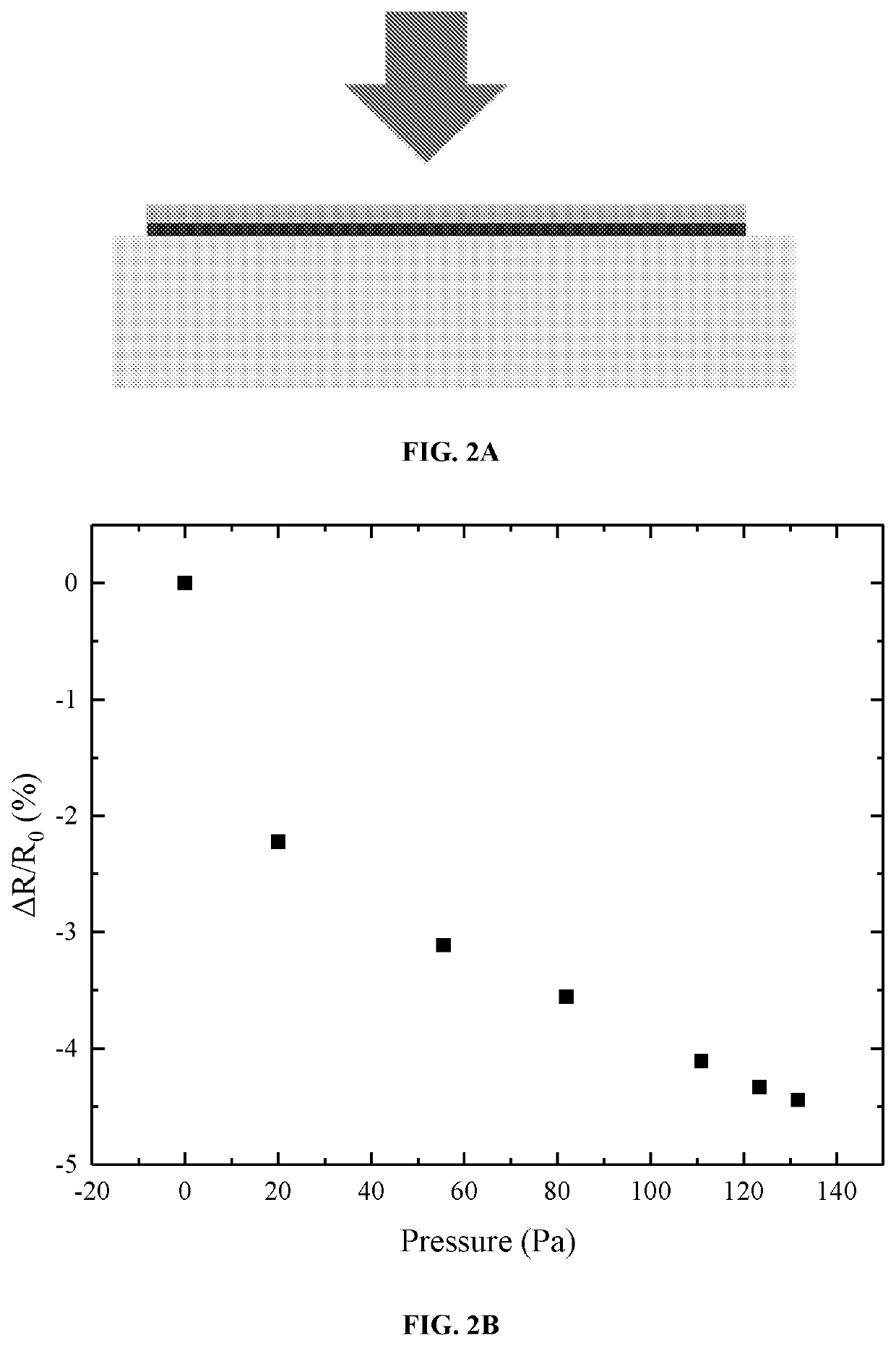
Measurement of Compressive Stress / Resistance (See FIG. 2):

[0131]Attach two strips of copper tape to two opposite corners of the film.[0132]Place film on a non-conductive surface.[0133]Connect the ends of each copper tape to the measurement device using wires and clips.[0134]Place small loads, ranging from 5 to 80 g on the film and record the corresponding value of resistance.

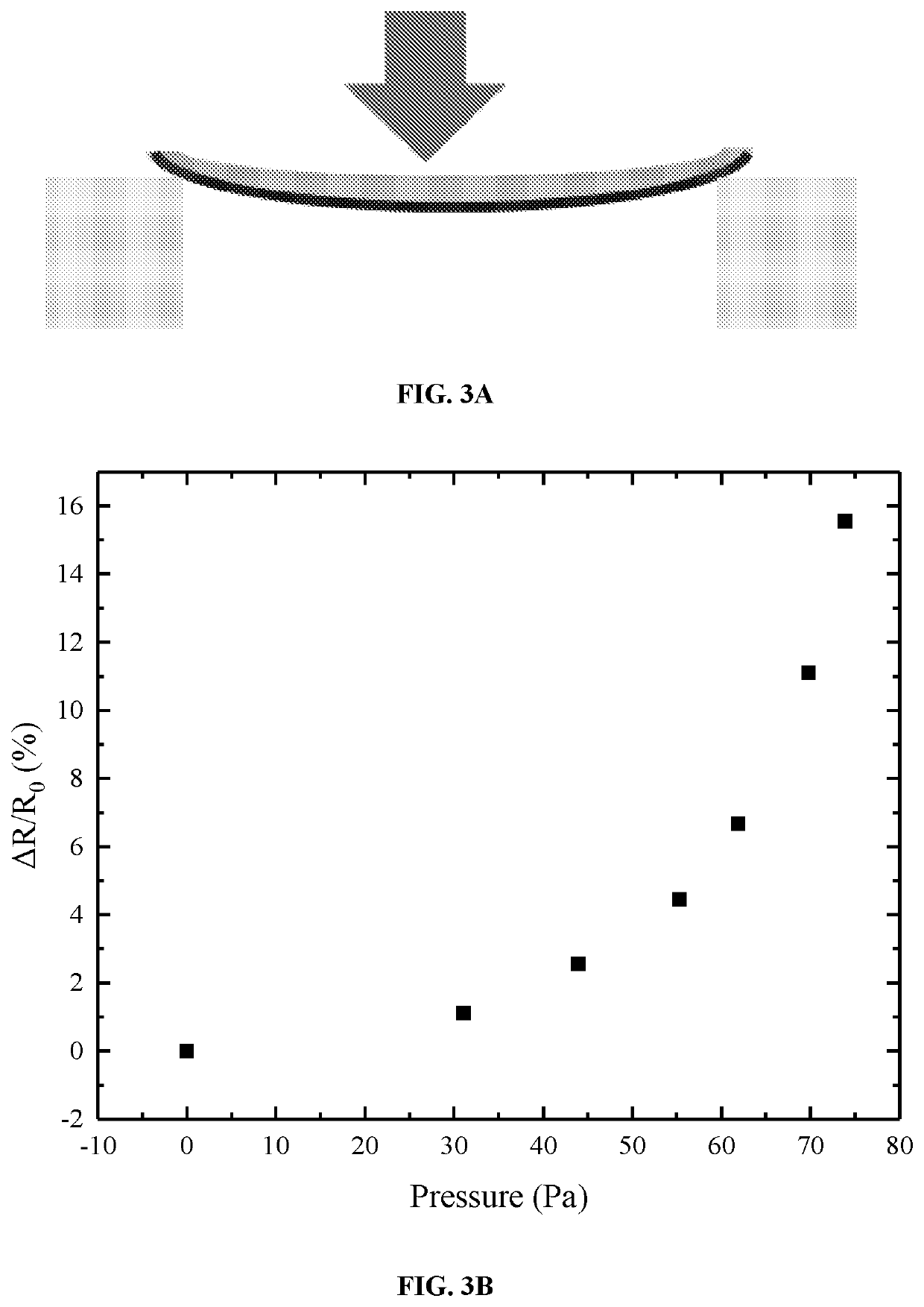
Measurement of Tensile Stress / Resistance (See FIG. 3):

[0135]Attach two strips of copper tape to two opposite corners of the film.[0136]Place the two corners of film onto two separated supporting surfaces, with the conductive side (black line in FIG. 3A) facing down.[0137]Connect the ends of each copper tape to the measurement device using wires and clips.[0138]Place small loads, ranging from 5 to 80 g on the...


PUM

PropertyMeasurementUnit
Fractionaaaaaaaaaa
Fractionaaaaaaaaaa
Fractionaaaaaaaaaa

Abstract

The invention relates to a force sensor which comprises a sensor material which comprises a plurality of metal nanowires dispersed within a matrix; and a measurement device configured to measure an electrical property of the sensor material, wherein the electrical property is one which changes in response to the application of a force to the sensor material.

Description

FIELD OF THE INVENTION[0001]The invention provides a force sensor comprising a sensor material and a measurement device. The invention also provides a force sensor comprising an array of sensor materials and at least one measurement device. The invention also provides a method for sensing force.BACKGROUND TO THE INVENTION[0002]This invention relates to the field of force sensing materials and force sensors, for instance devices for sensing pressure or strain. Such devices typically work by converting a force applied to the device into an electrical signal which can be detected. Traditionally, pressure sensors can generally be categorised as capacitive, piezoelectric or piezoresistive sensors.[0003]Firstly, capacitive pressure sensors typically consist of two conductive sheets of materials separated by a dielectric material (a parallel plate capactitor). When a pressure is applied, the distance between the conductive materials decreases and the resultant capacitance of the system cha...

Claims


Application Information

Patent Timeline
IPC IPC(8): G01L1/22C08J5/04C08J5/18G01L1/14B32B27/08B32B27/20B32B27/30
CPCG01L1/2287C08J5/041C08J5/18G01L1/146C08K2003/0806B32B27/20B32B27/306C08J2323/08B32B27/08G01L1/20G01L1/14B32B2262/103B32B5/145B32B7/02B32B7/022B32B2307/20B32B2307/30B32B2307/202B32B2457/00C08K2201/001C08K2201/011
Inventor LIU, WING CHUNGWATT, ANDREW
Owner OXFORD UNIV INNOVATION LTD
Learn More