Semiconductor laser diode and method for producing a semiconductor laser diode

a laser diode and semiconductor technology, applied in the direction of lasers, semiconductor devices, semiconductor lasers, etc., can solve the problems of disadvantage and low thermal conductivity, and achieve the effect of enhancing the electrical connection of the contact region

Pending Publication Date: 2022-04-28
OSRAM OPTO SEMICONDUCTORS GMBH
View PDF0 Cites 0 Cited by
  • Summary
  • Abstract
  • Description
  • Claims
  • Application Information

AI Technical Summary

Benefits of technology

The patent describes a semiconductor laser diode with a unique structure that allows for better control and performance. The diode includes a semiconductor layer sequence with a ridge and a damaged semiconductor structure, which can influence the active region and affect the current injection. The ridge is formed by removing a portion of the semiconductor layer sequence and the cover layer, and the cover layer is made of a transparent electrically conductive contact layer with higher electrical conductivity and lower electrical contact resistance than the cladding layer. The use of a transparent electrically conductive cover layer simplifies the manufacturing process and reduces costs. The technical effects of the patent include improved performance, simplified manufacturing process control, and better cost-effectiveness.

Problems solved by technology

In addition, the usual dielectric passivation materials, such as SiO2 or Si3N4, have only a low thermal conductivity, which can have a disadvantageous effect, especially when mounting such a laser diode with the passivated side on a carrier.

Method used


Image

  • Semiconductor laser diode and method for producing a semiconductor laser diode
  • Semiconductor laser diode and method for producing a semiconductor laser diode
  • Semiconductor laser diode and method for producing a semiconductor laser diode

Examples


Embodiment Construction

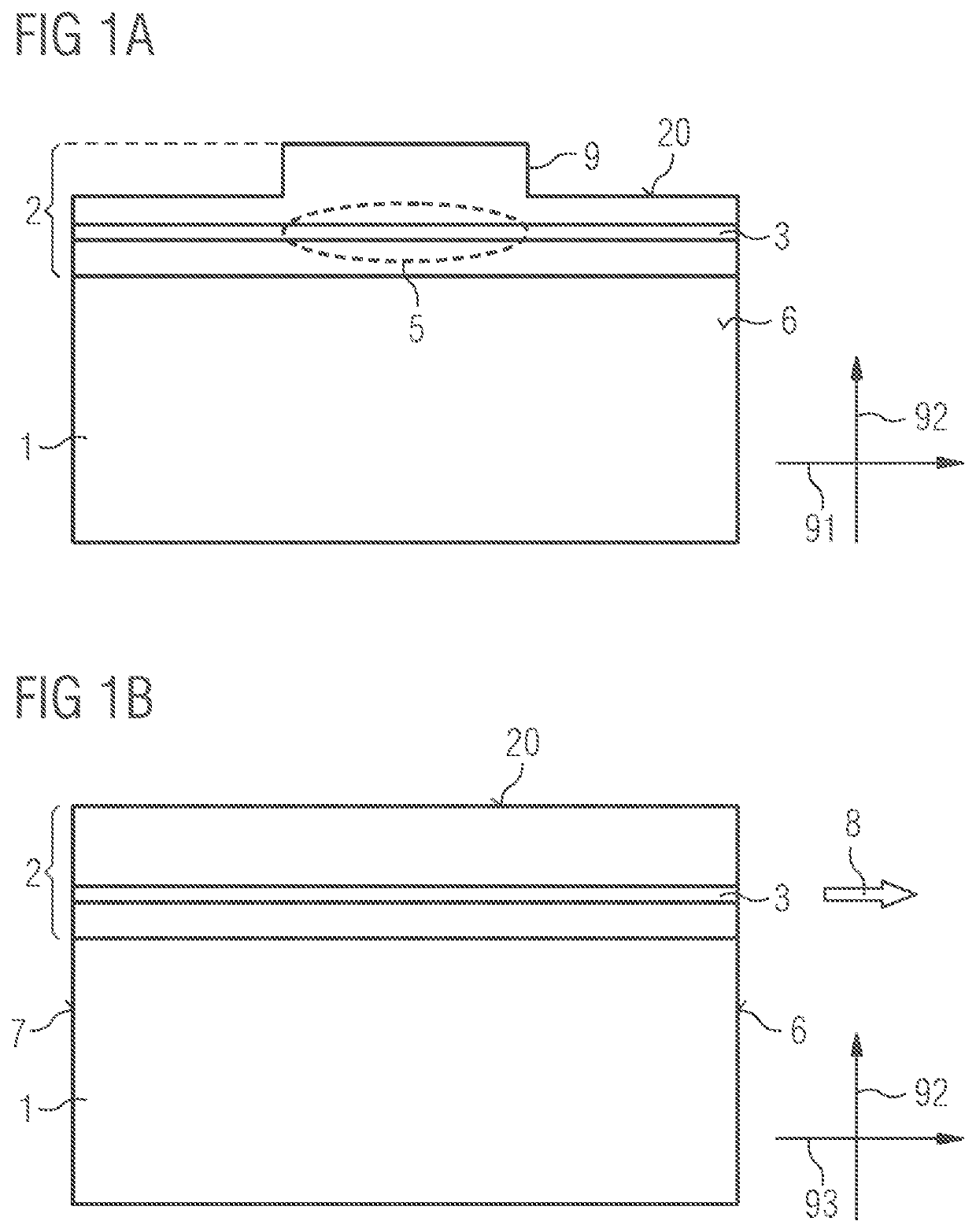
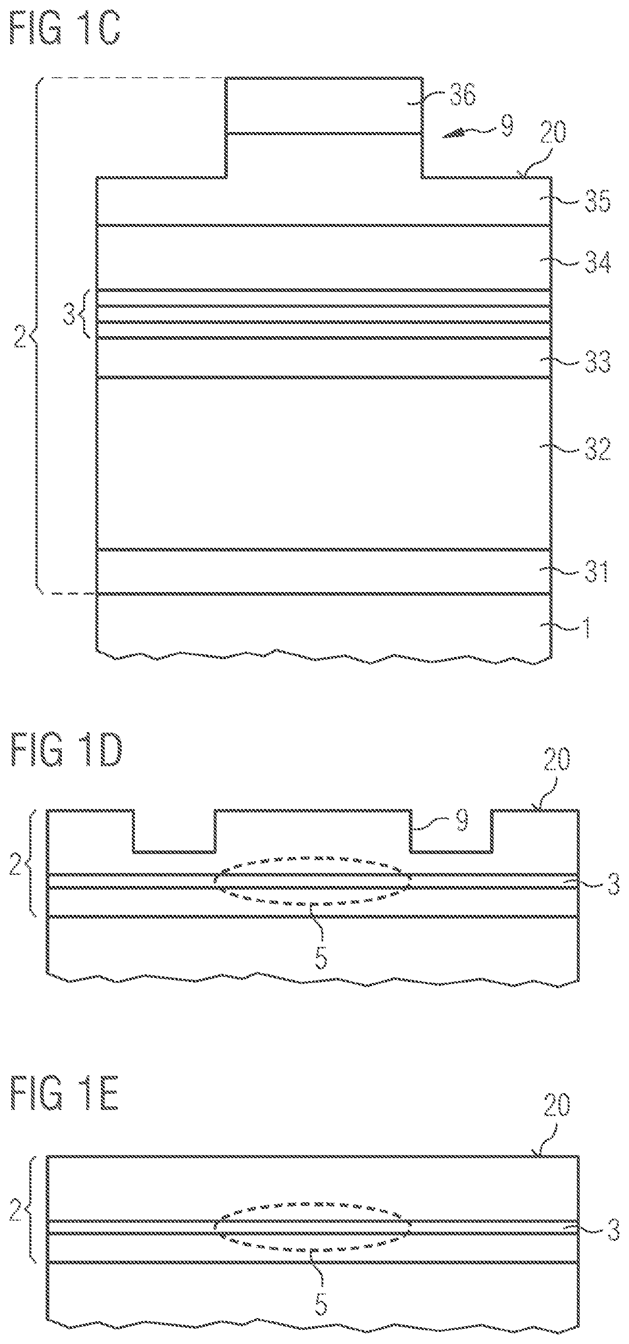
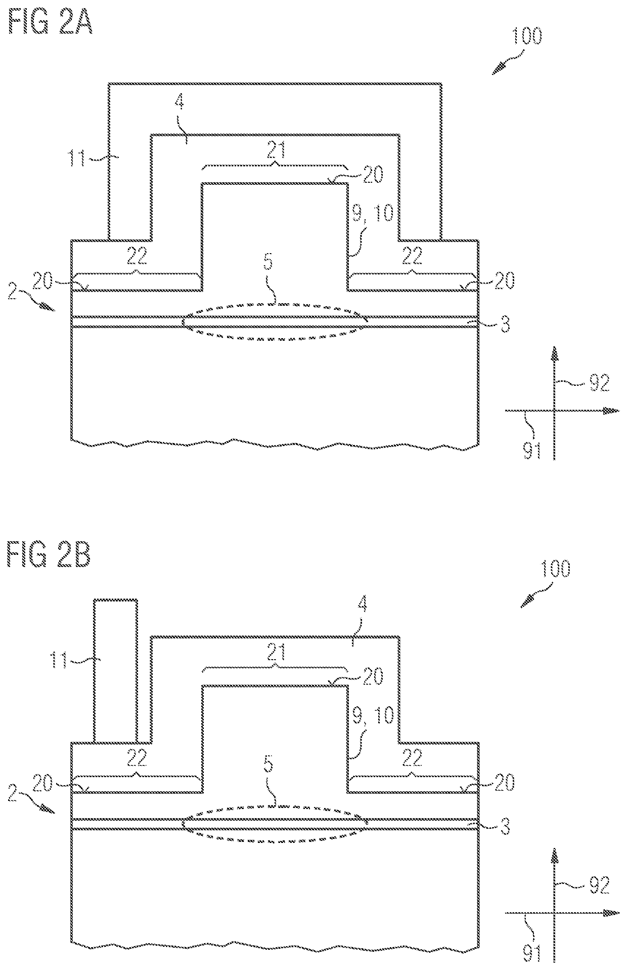
[0050]In the exemplary embodiments and figures, equal or similar elements or elements of equal function may each be designated with the same reference signs. The elements shown and their proportions to one another are not to be regarded as true to scale; rather, individual elements, such as layers, components, structural elements and areas, may be shown exaggeratedly large for better representability and / or for better understanding.

[0051]FIGS. 1A to 1E show exemplary embodiments of semiconductor layer sequences 2, each on a substrate 1, which are provided and used for the manufacture of the semiconductor laser diodes described below, where FIG. 1A shows a top view of the light outcoupling surface 6 of the later semiconductor laser diode and FIG. 1B shows a representation of a section through the semiconductor layer sequence 2 and the substrate 1 with a section plane perpendicular to the light outcoupling surface 6. FIG. 1C shows an exemplary embodiment of the structure of the semico...


PUM


Abstract

The invention relates to a semiconductor laser diode, which comprises a semiconductor layer sequence grown in a vertical direction and having an active layer that is configured and provided to generate light during operation in at least one active region extending in a longitudinal direction, and which comprises a transparent electrically conductive cover layer on the semiconductor layer sequence, wherein the semiconductor layer sequence terminates in a vertical direction with a top side, and the top side has a contact region arranged in the vertical direction above the active region and at least one cover region directly adjoining the contact region in a lateral direction perpendicular to the vertical and longitudinal directions, the cover layer is applied contiguously to the contact region and the at least one cover region on the top side, the cover layer is applied directly to the top side of the semiconductor layer sequence at least in the at least one cover region, and at least one element defining the at least one active region is present which is covered by the cover layer. The invention further relates to a method of manufacturing a semiconductor laser diode.

Description

CROSS-REFERENCE TO RELATED APPLICATIONS[0001]This patent application is a national stage entry from International Application No. PCT / EP2020 / 053776, filed on Feb. 13, 2020, published as International Publication No. WO 2020 / 182406 A1 on Sep. 17, 2020, and claims priority under 35 U.S.C. § 119 from German patent application 10 2019 106 536.4, filed Mar. 14, 2019, the disclosure content of all of which are hereby incorporated by reference.FIELD OF THE INVENTION[0002]A semiconductor laser diode and a method of manufacturing a semiconductor laser diode are specified.BACKGROUND OF THE INVENTION[0003]Commonly used laser diodes have, on the side facing away from the substrate, a dielectric passivation, which can also cover the side surfaces of a ridge waveguide structure depending on the laser diode design. After the ridge waveguide structure has been manufactured and overmolded with a passivation material, it must be removed again in the area where electrical contact is to be made. The st...

Claims


Application Information

Patent Timeline
IPC IPC(8): H01S5/042H01S5/22H01S5/343H01S5/026H01L33/62
CPCH01S5/04253H01S5/22H01L33/62H01S5/026H01S5/0421H01S5/34333H01S5/04256H01S5/4031H01S5/32341H01S5/3214H01S5/02476H01S5/2059H01S5/0234
Inventor GERHARD, SVENEICHLER, CHRISTOPHLELL, ALFREDALI, MUHAMMAD
Owner OSRAM OPTO SEMICONDUCTORS GMBH
Why Eureka
Try Eureka