
METAL AND TIN ALLOY HAVING LOW alpha-RAY EMISSION, AND METHOD FOR PRODUCING SAME

Inactive Publication Date: 2020-12-10
MITSUBISHI MATERIALS CORP
View PDF0 Cites 0 Cited by
  • Summary
  • Abstract
  • Description
  • Claims
  • Application Information

AI Technical Summary

Benefits of technology

The present invention relates to metals and tin alloys with low α-ray emission, which can be used as solder materials in semiconductor devices. The metals and tin alloys have a characteristic of low α-ray emission even after production and heating at 100°C for six hours. The low α-ray emission is important for reducing the possibility of soft errors in the semiconductor device. The invention also provides a method for decreasing the concentration of 210Pb, which is a parent nuclide that causes α-ray emission, in the metallic raw material. The method involves turning the metallic raw material into a tin sulfate aqueous solution and removing lead sulfate from the solution using a lead nitrate aqueous solution with low α-ray emission. The resulting metal or tin alloy has low α-ray emission and can be used as a solder material in semiconductor devices without causing soft errors.

Problems solved by technology

Even for Pb-free solder materials, it is extremely difficult to completely remove Pb from Sn which is a principal solder material, and a small amount of Pb is included in Sn as an impurity.
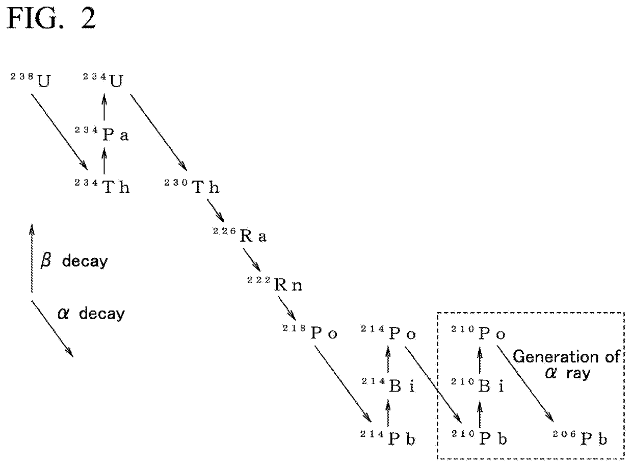
In recent years, it has been found that, in semiconductor devices having a density and a capacity that are increasing more and more, an a ray that is emitted from 210Po generated from 210Pb which is an isotope of Pb is one cause for the generation of a soft error.
Meanwhile, in recent years, there has been a report regarding a problem with the generation rate of a soft error which increases when a chip joined to a substrate by soldering is exposed to a high-temperature environment during use compared with that in the initial phase of use (for example, refer to NPL 1 (Abstract)).

Method used


Image

  • METAL AND TIN ALLOY HAVING LOW alpha-RAY EMISSION, AND METHOD FOR PRODUCING SAME
  • METAL AND TIN ALLOY HAVING LOW alpha-RAY EMISSION, AND METHOD FOR PRODUCING SAME
  • METAL AND TIN ALLOY HAVING LOW alpha-RAY EMISSION, AND METHOD FOR PRODUCING SAME

Examples


first embodiment

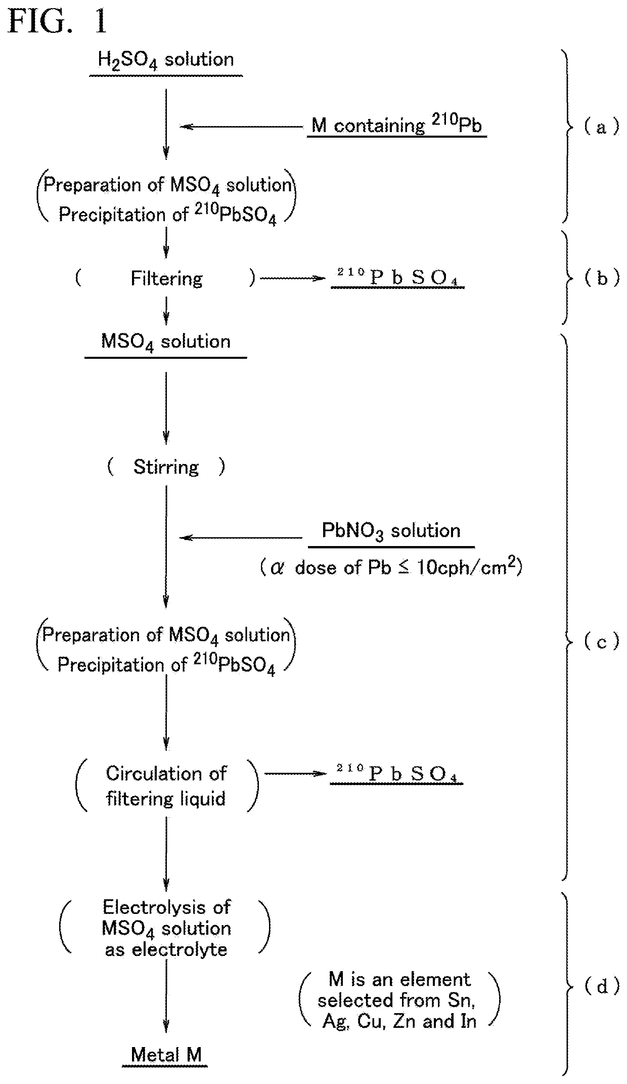
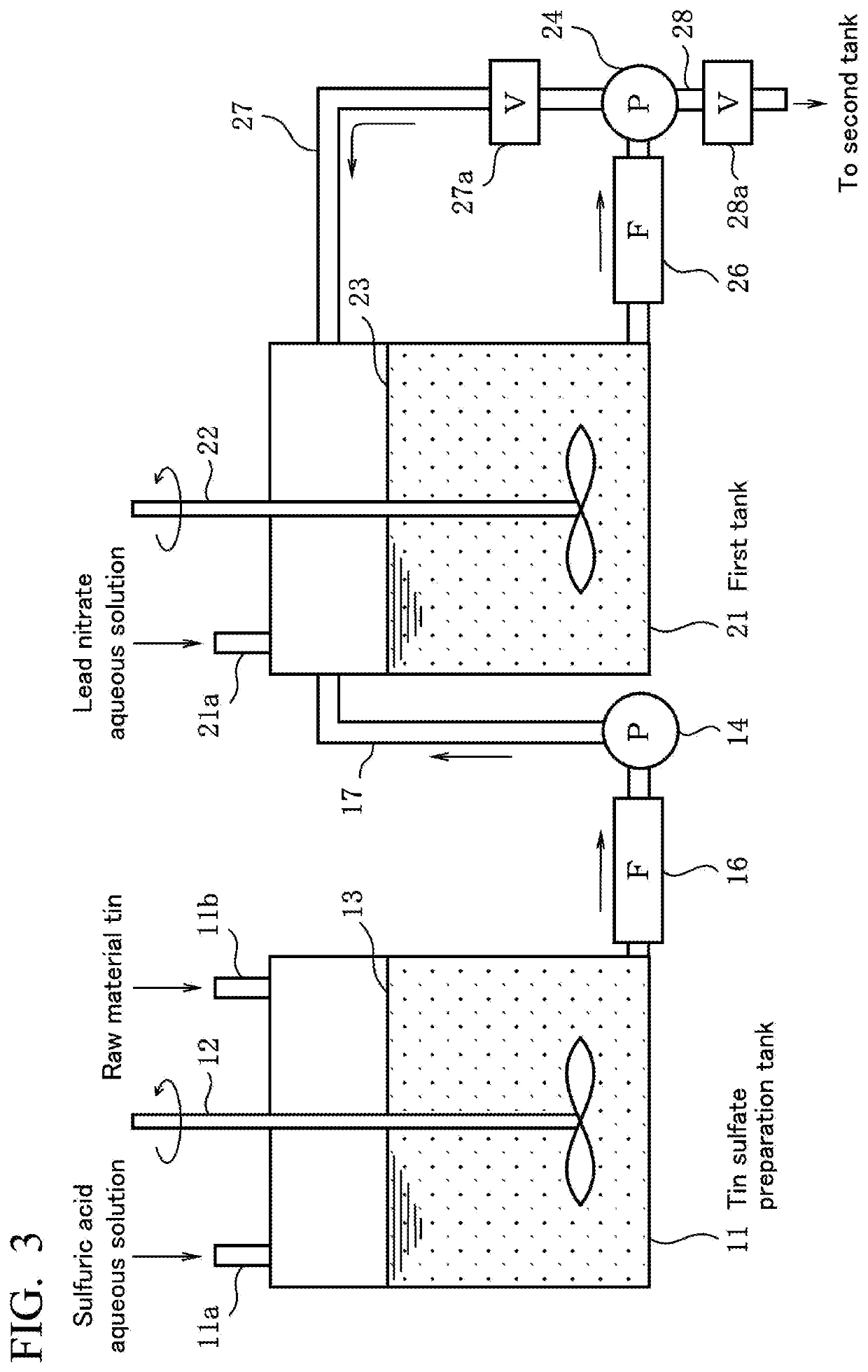
[0055]First, a method for producing any metal having a low α-ray emission of tin, silver, copper, zinc, and indium (metallic material for a solder material) of a first embodiment of the present invention will be described in an order of steps shown in FIG. 1 or on the basis of a production apparatus shown in FIG. 3.

Step (a) and Step (b)

Metallic Raw Material

[0056]Regarding a metallic raw material for obtaining any metal having a low α-ray emission of tin, silver, copper, zinc, and indium (represented by M in FIG. 1) of the first embodiment, the selection of the metallic raw material is not restricted by the degree of the content of Pb as an impurity or the α-ray emission.

[0057]For example, even when a metal such as commercially available tin including Pb at a concentration of approximately 320 mass-ppm and an α-ray emission by Pb being approximately 9 cph / cm2 is used as the metallic raw material, in the metal that is obtained in the end using a production method and a production appa...

second embodiment

[0081]Next, a method for producing a tin alloy having a low α-ray emission of a second embodiment of the present invention will be described.

[0082]In this production method, a tin alloy is produced by casting metallic tin (Sn) having a low α-ray emission obtained in the first embodiment and one or more kinds of metals selected from a group consisting of silver, copper, zinc, indium, bismuth, nickel, and germanium.

[0083]Here, as the metal that forms an alloy with the metallic tin, in the case of using the tin alloy as a solder, silver, copper, zinc, and indium are preferred from the viewpoint of the dissolving point and mechanical characteristics of the solder. In order to attain the object of the present invention, the α-ray emission of silver, copper, zinc, indium, bismuth, or nickel that forms an alloy with the metallic tin is 0.002 cph / cm2 or less.

[0084]In the present embodiment, for the casting, it is possible to use a furnace that is generally used for casting, for example, a h...

example 1

[0087]As a metallic raw material, commercially available Sn powder having an α-ray emission of 10.2 cph / cm2 and a concentration of Pb being 15 ppm was used, and this metallic raw material was added to and mixed with a sulfuric acid aqueous solution having a concentration of 130 g / L stored in a tin sulfate preparation tank and dissolved at 50° C., thereby preparing 200 g / L of a tin sulfate aqueous solution 1 m3. Therefore, Pb contained in the tin that was the metallic raw material was precipitated in a form of lead sulfate. The tin sulfate aqueous solution was filtered by being passed through a membrane filter (pore diameter: 0.2 μm) manufactured by Yuasa Membrane Systems Co., Ltd., thereby removing lead sulfate.

[0088]Next, in a first tank, while stirring the tin sulfate aqueous solution from which lead sulfate has been removed at a rotation rate of 100 rpm, a lead nitrate aqueous solution (the concentration of lead nitrate: 20% by mass) including Pb having an α-ray emission of 5 cph...


PUM

PropertyMeasurementUnit
Temperatureaaaaaaaaaa
Timeaaaaaaaaaa

Abstract

Any metal having a low α-ray emission, the metal being any one of tin, silver, copper, zinc, or indium, wherein an emission of an α-ray after heating the metal at 100° C. in an atmosphere for six hours is 0.002 cph / cm2 or less. Any metal of tin, silver, copper, zinc and indium each including lead as an impurity is dissolved to prepare a hydrosulfate aqueous solution of the metal and lead sulfate is precipitated and removed in the solution. The lead sulfate is precipitated in the hydrosulfate aqueous solution by adding a lead nitrate aqueous solution including lead having an a-ray emission of 10 cph / cm2 or less to the hydrosulfate aqueous solution, from which the lead sulfate has been removed, and, at the same time, the solution is circulated while removing the lead sulfate to electrowinning the metal using the hydrosulfate aqueous solution as an electrolytic solution.

Description

TECHNICAL FIELD[0001]The present invention relates to any metal having a low a-ray emission of tin, silver, copper, zinc, or indium which is preferred for a solder material for producing electronic components and has an extremely small a-ray emission. In addition, the present invention relates to an alloy having a low a-ray emission of one or more metals selected from a group consisting of silver, copper, zinc, indium, bismuth, nickel, and germanium and tin (hereinafter, referred to as the tin alloy). Furthermore, the present invention relates to each method for producing the metal or the tin alloy having a low α-ray emission.[0002]Priority is claimed on Japanese Patent Application No. 2017-157394, filed on Aug. 17, 2017 and Japanese Patent Application No. 2018-142195, filed on Jul. 30, 2018, the contents of which are incorporated herein by reference.BACKGROUND ART[0003]As solder materials for producing electronic components, development of solder materials containing Pb-free tin (S...

Claims


Application Information

Patent Timeline
IPC IPC(8): C22C13/00B23K35/26C22B25/08C25C1/14C25C1/12C25C1/16C25C1/20C25C1/22C22B13/08
CPCC25C1/12C22B25/08C25C1/22C22C2202/00C25C1/16C22C13/00B23K2101/40C22B13/08B23K35/262C25C1/14C25C1/20C22B11/00C22B19/32C22B58/00
Inventor HIRANO, HIROTAKAYOSHIDA, YOSHIHIROKATASE, TAKUMA
Owner MITSUBISHI MATERIALS CORP
Learn More