Surface-treated material and component produced by using the same

a technology of surface treatment and surface treatment, which is applied in the direction of contact member manufacturing, liquid/solution decomposition chemical coating, capacitors, etc., can solve the problems of difficult formation of a plating film with adequate adhesiveness of aluminum, complicated method of aluminum surface plating, and difficulty in a base metal such as aluminum to be plated in a wet process. , to achieve the effect of safe production, simple process and low cos

Inactive Publication Date: 2019-10-24
FURUKAWA ELECTRIC CO LTD
View PDF5 Cites 2 Cited by
  • Summary
  • Abstract
  • Description
  • Claims
  • Application Information

AI Technical Summary

Benefits of technology

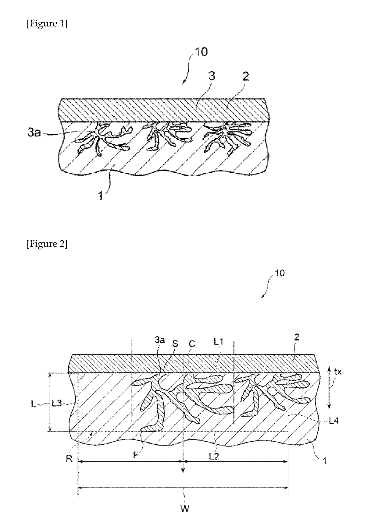
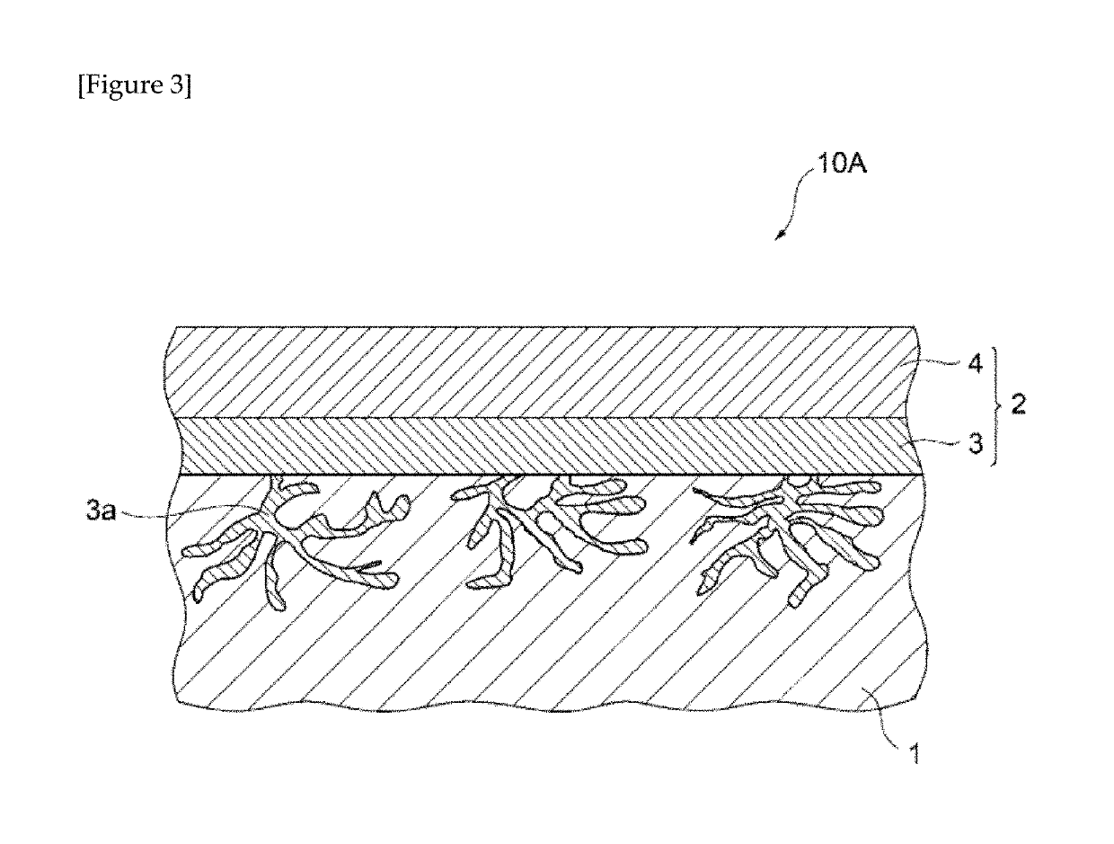
[0028]According to the present invention, a surface-treated material is provided that comprises an electroconductive substrate, in particular, an electroconductive substrate which is, for instance, aluminum or an aluminum alloy which is mainly formed of a base metal having a large ionization tendency and is considered to resist having a sound plating film formed thereon, and a surface treatment film that is formed of at least one or more layers of metal layers which are formed on the electroconductive substrate, wherein among the at least one or more layers of metal layers, the lowermost metal layer which is a metal layer directly formed on the electroconductive substrate comprises a plurality of metal-buried portions that are scattered in the electroconductive substrate, branch from the surface of the electroconductive substrate and widely extend toward the inside thereof. In addition, according to the present invention, a surface-treated material is provided that comprises an electroconductive substrate and a surface treatment film formed of one or more layers of metal layers on the electroconductive substrate, wherein among the metal layers forming the surface treatment film, the lowermost metal layer in contact with the electroconductive substrate comprises a plurality of metal-buried portions that branch from the surface of the electroconductive substrate and widely extend toward the inside thereof. Thereby, it becomes possible to provide a surface-treated material that simplifies its process, as compared to a conventional surface-treated material in which a zinc-containing layer (in particular, zincate treatment layer) having a thickness, for instance, of approximately 100 nm is interposed between the substrate and the plating film, and as a result, can be safely produced at an inexpensive cost; in addition, exhibits excellent adhesiveness as a result of the metal-buried portions of the lowermost metal layer infiltrating into the inside of the electroconductive substrate to thereby provide a mechanical anchoring effect; and further can greatly shorten its production time period.
[0030]In the present invention, it becomes possible to provide a surface-treated material that exhibits adequate adhesiveness as a result of the metal-buried portion of the lowermost metal layer infiltrating into the inside of the electroconductive substrate to thereby provide a mechanical anchoring effect and further can greatly shorten its production time period, by having the above described features. In addition, a surface-treated material can be provided in which the metal-buried portion of the lowermost metal layer branches from the surface of the electroconductive substrate and widely extends toward the inside thereof, and accordingly the branching portion is more strongly buried in the inside of the electroconductive substrate, and that exhibits more excellent adhesiveness. In addition, the area ratio of the metal-buried portion which adheres to (contacts) the electroconductive substrate is in the range of 5% or more and 50% or less in the predetermined observation region of the electroconductive substrate; thereby the metal-buried portion can keep an appropriate mechanical anchoring effect, while infiltrating the metal of the metal-buried portion from any of a crystal grain boundary and an inside of the crystal grain; and as a result, a surface-treated material excellent in both characteristics of the bending workability and the adhesiveness can be provided. Such a surface-treated material can keep the original characteristics which are obtained after the surface treatment film has been formed without deteriorating them in use environment, for instance, at high temperature (for instance, approximately 200° C.); and accordingly it has become possible to provide a surface-treated material having high long-term reliability, and various components, for instance, terminals, connectors, bus bars, lead frames, medical members, shield cases, coils, contact switches, cables, heat pipes, memory disks and the like, which are produced by using the same.

Problems solved by technology

By the way, it is considered that a method of plating the surface of the aluminum is complicated which is referred to as a light metal among metals, and besides that it is difficult for aluminum to have a plating film with adequate adhesiveness formed thereon.
Examples of factors for this include the following: aluminum is apt to have an oxide film called a passivation film formed on its surface, this oxide film exists in a stable state, and it is difficult for a base metal such as aluminum to be plated in a wet process.
In addition, in the case where an underlying layer such as a nickel layer which is formed for the purpose of improving plating adhesiveness and a coating layer which is formed of a metal (tin, silver and the like) for electric contact are sequentially formed on the surface of an aluminum-based base material, for instance, by a wet plating method, even if the underlying layer is formed on the surface of the base material and then the coating layer is formed on the underlying layer, sufficient adhesiveness cannot be usually obtained due to an oxide film present on the surface of the base material.
However, there has been a problem that bending workability deteriorates because the unevenness of 5 to 10 μm becomes a stress concentration point at the time of deformation.
As a result, the plating layer results in causing various problems: for example, a contact resistance results in increasing, wire bonding properties are lowered and solder wettability is lowered.
In addition, in some state of the zinc layer formed in the zincate treatment, there have been cases where plating defects often occur such as the formation of bumps in the subsequent plating and precipitation abnormality.
However, if the plating layer (underlying layer) which is formed after the zinc substitution treatment is thinly formed, it is difficult to completely coat the zinc-containing layer due to the formation of a nonuniform plating layer and the formation of pinholes, and there is a problem that erosion preferentially proceeds along the zinc-containing layer in the salt water environment, and that as a result, peeling occurs between the underlying layer and the base material.
As for a method of plating an aluminum base material without through the zinc layer, for instance, the electroless nickel is proposed which uses a hydrofluoric acid and / or a salt thereof and a nickel salt (for instance, Patent Literature 5); but nickel precipitates disorderly, mismatch among lattices becomes large, and accordingly sufficient adhesiveness could not be obtained.
However, the nickel-based plating layer is usually harder than the aluminum-based base material, and accordingly there are problems that if the thickness of the nickel-based plating layer is formed excessively thick in order to inhibit the diffusion of zinc, the nickel-based plating layer (film) cannot follow the deformation of the aluminum-based base material, when a bending work has been applied to the plating layer in a step of producing a terminal, cracks easily occur, and corrosion resistance is also inferior.
Furthermore, in recent years, the miniaturization of electronic components and the like has progressed, and bendability under severer conditions is required.
When the conductors are subjected to a bending work which does not change the inner bending radius, the conductor having a larger cross-sectional area results in showing a larger tensile strain on the outer side of the bent part, and tends to easily cause cracks on the plating surface.
In these applications, the following problem has also arisen: cracks result in occurring when the nickel-based plating which has been used for inhibiting the diffusion of zinc has a conventional thickness.

Method used


Image

  • Surface-treated material and component produced by using the same
  • Surface-treated material and component produced by using the same
  • Surface-treated material and component produced by using the same

Examples


example 1

Conventional Example 1

[0078]In Conventional Example 1, the electrolytic degreasing step was conducted on the aluminum base material (size of 0.2 mm×30 mm×30 mm) shown in Table 11 under the above described conditions; and then a conventional zinc substitution treatment (zincate treatment) was conducted, and thereby the zinc-containing layer having a thickness of 110 nm was formed. After that, the surface activation treatment was not conducted, and the surface treatment film was formed that was formed of two layers of the metal layers which were formed of the nickel plating layer and the gold plating layer so that the thickness shown in Table 11 was obtained, by the above described surface treatment film forming step; and the surface-treated material was prepared.

example 2

Conventional Example 2

[0079]Conventional Example 2 is a surface-treated material which was prepared by forming the surface treatment film on the base material, while referring to and simulating examples of Patent Literature 4. An aluminum base material was prepared which was pretreated by etching treatment by an operation of: conducting the electrolytic degreasing step on the aluminum base material (size of 0.2 mm×30 mm×30 mm) shown in Table 11 under the above described conditions; and then immersing the aluminum base material in an etching solution that was obtained by diluting “NAS-727” (of which main component is 18% hydrochloric acid)” which was an active acid solution containing hydrochloric acid as a main component and was made and sold by Sunlight Corporation, into double volume, at a temperature of 35° C. for 2 minutes. After that, the surface of the pretreated aluminum substrate was subjected to surface activation treatment. The surface activation treatment was conducted wi...


PUM

PropertyMeasurementUnit
widthaaaaaaaaaa
depthaaaaaaaaaa
thicknessaaaaaaaaaa

Abstract

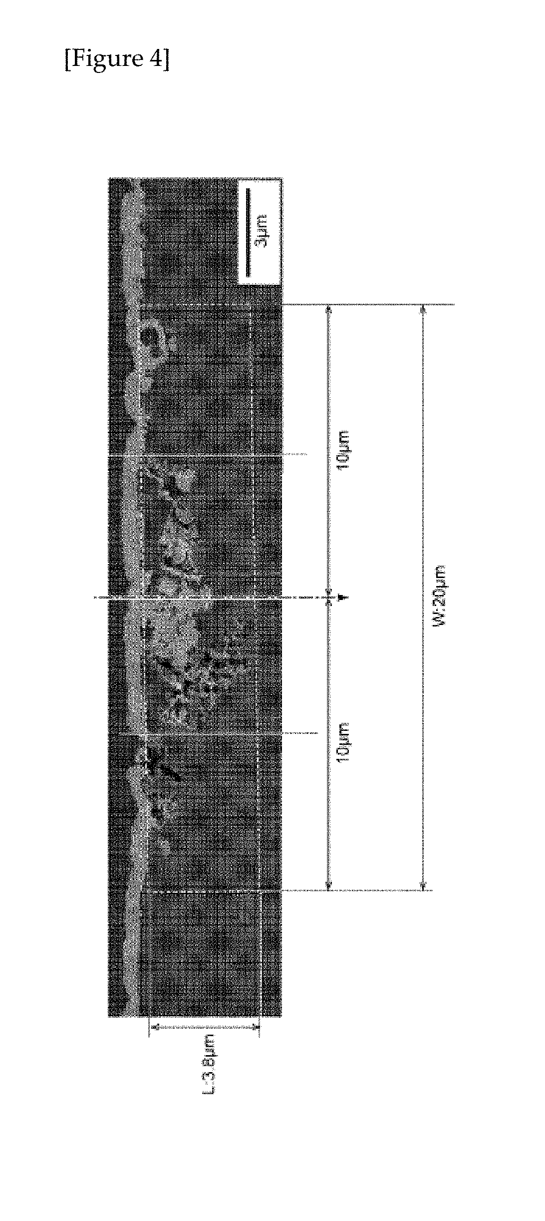
A surface-treated material (10) according to the present invention comprises an electroconductive substrate (1) and a surface treatment film (2) formed of at least one or more layers of metal layers (3 and 4) which are formed on the electroconductive substrate (1), wherein among the at least one or more layers of metal layers (3 and 4), the lowermost metal layer (3) which is directly formed on the electroconductive substrate (1) comprises a plurality of metal-buried portions (3a) that are scattered in the electroconductive substrate (1), branch from a surface of the electroconductive substrate (1) and widely extend toward the inside thereof, and as a vertical cross section of the surface-treated material (10) is viewed, in which at least one of the metal-buried portions (3a) exists in the electroconductive substrate (1), an average value of an area ratio of the metal-buried portion (3a) occupying the predetermined observation region of the electroconductive substrate (1) is in a range of 5% or more and 50% or less.

Description

TECHNICAL FIELD[0001]The present invention relates to a surface-treated material and a component produced by using the same, and particularly relates to a technology that simply forms a surface treatment film that is formed of at least one layer of a metal layer and has an adequate adhesiveness, on an electroconductive substrate which is mainly formed of a base metal having a large ionization tendency and is considered to resist having a sound plating film formed thereon.BACKGROUND ART[0002]For a material to be plated (electroconductive substrate) which is used for forming a conventional electrical contact and the like, metal materials such as copper, copper alloys, iron and iron alloys have been widely used, from the viewpoint of being inexpensive and having comparatively excellent characteristics. Because such metal materials are satisfactory particularly in electroconductivity and workability, are easily available, in addition, can easily have coating treatment applied on their s...

Claims


Application Information

Patent Timeline
Patent Type & Authority Applications(United States)
IPC IPC(8): C25D7/00H01B1/02C25D5/12C25D5/44C25D3/12C25D3/38
CPCC25D3/38C25D7/00H01B1/023C25D3/12C25D5/44C25D5/12H01B1/02H01R13/03H01R43/16C25D5/10C25D5/50C25D5/617C23C18/1653C23C18/1831
Inventor KOBAYASHI, YOSHIAKIYAMAUCHI, MIHO
Owner FURUKAWA ELECTRIC CO LTD
Why Eureka
Try Eureka