
Method for growing gallium nitride based on graphene and magnetron sputtered aluminium nitride

a gallium nitride and graphene technology, applied in the field of microelectronics technology, can solve the problems of high dislocation density, limited performance and reliability of gallium nitride-based devices, and use of silicon carbide as the substrate which has too high cost, so as to improve the quality of gallium nitride film

Active Publication Date: 2019-04-11
XIDIAN UNIV
View PDF0 Cites 6 Cited by
  • Summary
  • Abstract
  • Description
  • Claims
  • Application Information

AI Technical Summary

Benefits of technology

This patent describes a new way to grow high quality gallium nitride films using graphene and magnetron sputtering aluminum nitride technology. This can improve the quality of the film and make it easier to produce.

Problems solved by technology

However, due to the large lattice mismatch and thermal mismatch between a gallium nitride material and a substrate, the gallium nitride obtained by heteroepitaxial tends to have very high dislocation density, which greatly limits the performance and reliability of gallium nitride-based devices.
However, deficiencies of this method are as follows.
Firstly, the method uses silicon carbide as the substrate which has too high cost.
Secondly, in this method, the graphene is directly grown on the silicon carbide substrate.
The growth is difficult and the quality of the graphene is poor.
Thirdly, in this method, the thin layer of nitride is directly inserted between the graphene layer and the gallium nitride layer; it is difficult for the thin layer of nitride to nucleate, and the crystal quality is poor, which affects the growth of gallium nitride in the next process.
However, deficiencies of this method are as follows.
Firstly, since the method comprises epitaxial growing on a copper substrate, the temperature of the subsequently grown nitride material cannot be higher than the melting point of copper.
Thus, the better AlN layer cannot be grown in the method and the quality of obtained nitride material is poor.
Secondly, the method does not use a transition layer; and the nitride material can only be grown on the substrate with small lattice mismatch.

Method used


Image

  • Method for growing gallium nitride based on graphene and magnetron sputtered aluminium nitride
  • Method for growing gallium nitride based on graphene and magnetron sputtered aluminium nitride
  • Method for growing gallium nitride based on graphene and magnetron sputtered aluminium nitride

Examples


first embodiment

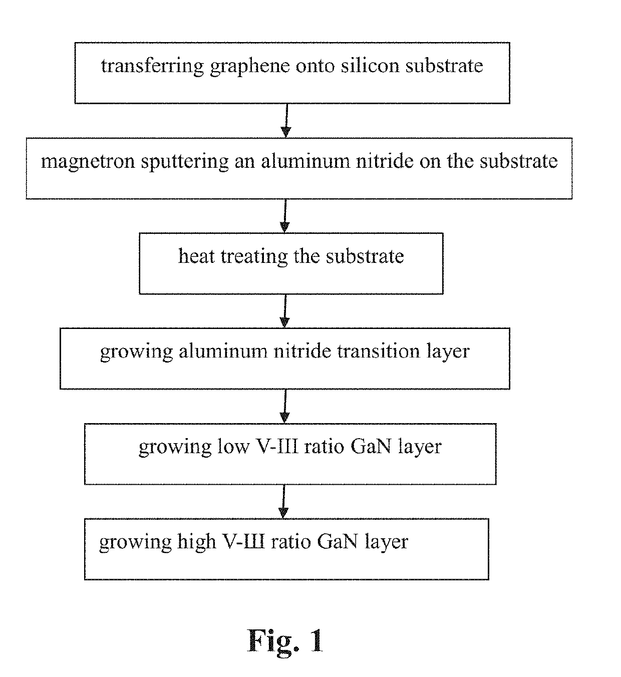
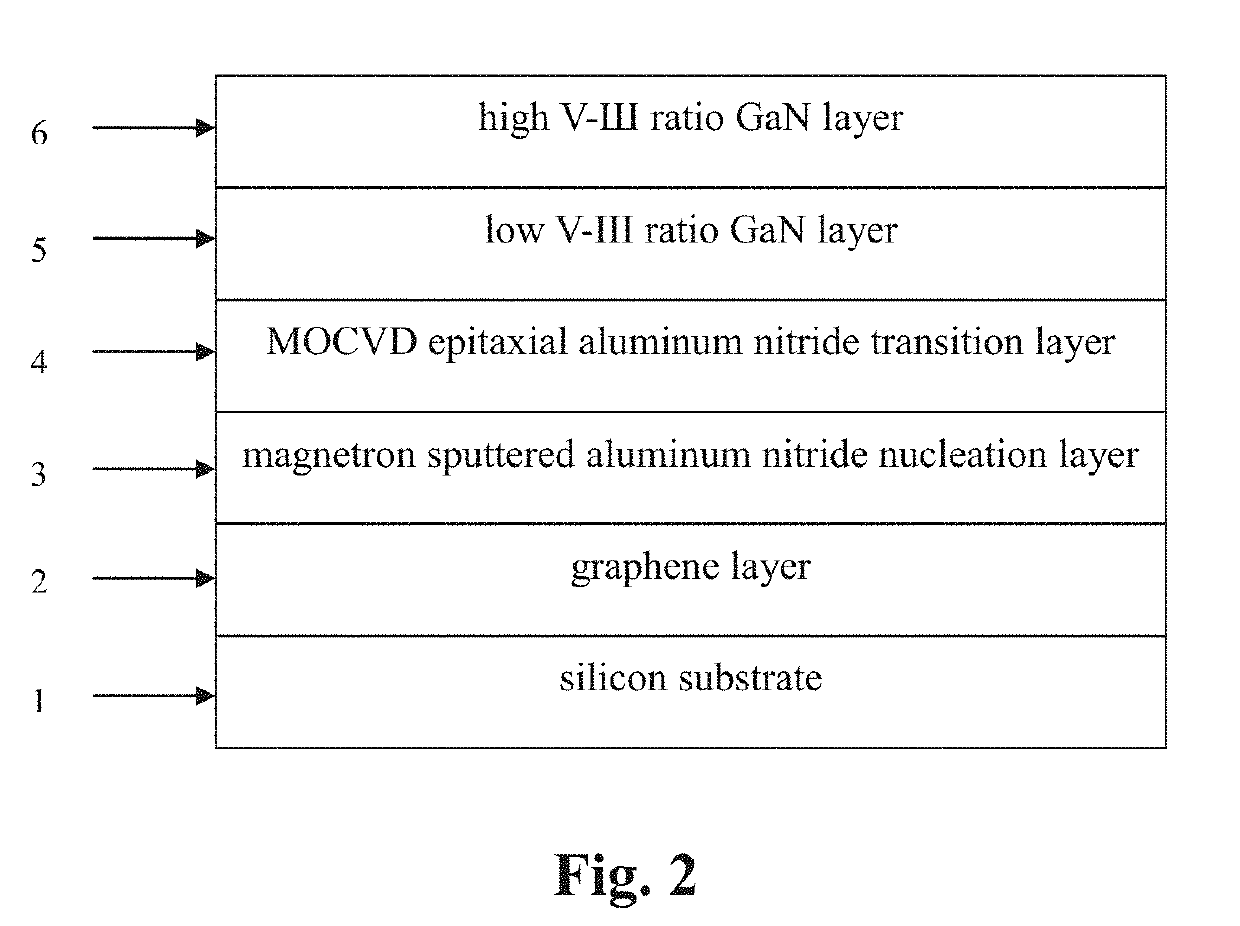
[0016]Referring to FIG. 1, the method of the first embodiment utilizes a silicon substrate and graphene, and forms an aluminum nitride nucleation layer by magnetron sputtering, and uses a pulsed metal organic chemical vapor deposition (MOCVD) method for epitaxial growth of aluminum nitride. Specifically, firstly, a single layer of graphene is transferred onto a silicon substrate; then, a layer of aluminum nitride nucleation layer is magnetron sputtered, which is used for alleviating the stress caused by lattice mismatch between the silicon substrate and the gallium nitride; next, the MOCVD reaction chamber and a pulse method are used for epitaxial growth of a layer of aluminum nitride as a transition layer, to improve the quality of the material; finally, the sample is placed in the MOCVD reaction chamber for sequentially epitaxial growth of the aluminum nitride transition layer, a low V-III ratio GaN epitaxial layer and a high V-III ratio GaN epitaxial layer. The quality of gallium...

second embodiment

[0035]The method of the second embodiment utilizes a sapphire substrate. In the method of the second embodiment, firstly, a single layer of graphene is transferred onto the sapphire substrate, such that the temperature of the subsequently grown nitride material depends on the temperature of the sapphire substrate; then, a layer of aluminum nitride film is magnetron sputtered, which is used for alleviating the stress caused by lattice mismatch between the substrate and the gallium nitride; next, a layer of aluminum nitride film is epitaxially grown as a transition layer by using MOCVD method, to improve the quality of the material; finally, the sample is placed in MOCVD reaction chamber; and sequentially, the aluminum nitride transition layer, the low V-III ratio GaN epitaxial layer and the high V-III ratio GaN epitaxial layer are epitaxially grown. The quality of gallium nitride can be further improved by adjusting the pressure, flow rate, temperature and thickness growth conditions...

third embodiment

[0054]In the method of the third embodiment, firstly, a layer of graphene is grown on a copper substrate; then, a layer of aluminum nitride film is magnetron sputtered, which is used for alleviating the stress caused by lattice mismatch between the substrate and the gallium nitride; finally, the sample is placed in MOCVD reaction chamber; and, sequentially, an aluminum nitride transition layer, a low V-III ratio GaN epitaxial layer and a high V-III ratio GaN epitaxial layer are epitaxially grown. The quality of gallium nitride can be further improved by adjusting the pressure, flow rate, temperature, and thickness growth conditions during growth of each layer.

[0055]Referring to FIG. 5, the method of this embodiment includes the follow steps:

[0056]Step 1: Growing Graphene.

[0057]Firstly, a cleaned copper foil is placed in a tubular furnace quartz tube; the tubular furnace quartz is vacuumized for 10 minutes; then, hydrogen gas is introduced therein; the tube furnace is heated to 1000°...


PUM

PropertyMeasurementUnit
Temperatureaaaaaaaaaa
Timeaaaaaaaaaa
Thicknessaaaaaaaaaa

Abstract

The present invention discloses a method for growing gallium nitride based on graphene and magnetron sputtered aluminum nitride, and a gallium nitride thin film. The method according to an embodiment comprises: spreading graphene over a substrate; magnetron sputtering an aluminum nitrite onto the graphene-coated substrate to obtain a substrate sputtered with aluminum nitrite; placing the substrate sputtered with aluminum nitride into a MOCVD reaction chamber and heat treating the substrate to obtain a heat treated substrate; growing an aluminum nitride transition layer on the heat treated substrate and a first and a second gallium nitride layer having different V-III ratios, respectively. The gallium nitrate thin film according to an embodiment comprises the following structures in order from bottom to top: a substrate (1), a graphene layer (2), an aluminum nitride nucleation layer (3) fabricated by using a magnetron sputtering method, an aluminum nitride transition layer (4) grown by MOCVD, and a first and a second gallium nitrate layer (5, 6) having different V-III ratios.

Description

TECHNICAL FIELD[0001]The invention belongs to the field of microelectronics technology, and, more particularly, relates to a method for growing gallium nitride which can be used for fabricating a semiconductor device.BACKGROUND[0002]The third-generation wide bandgap semiconductor materials, typically including gallium nitride (GaN), have wide applications in the field of optoelectronic devices and electronic devices due to their wide bandgap, high electron mobility and high breakdown field. The growth of high-quality gallium nitride is the key to making microwave power devices. However, due to the large lattice mismatch and thermal mismatch between a gallium nitride material and a substrate, the gallium nitride obtained by heteroepitaxial tends to have very high dislocation density, which greatly limits the performance and reliability of gallium nitride-based devices. Therefore, epitaxial growth of gallium nitride materials with low dislocation density is a key technology in GaN res...

Claims


Application Information

Patent Timeline
IPC IPC(8): H01L21/02H01L29/20C30B25/18C30B29/40C23C14/06C23C16/30C23C16/02C23C14/35
CPCH01L21/02444H01L21/02381H01L21/0242H01L21/02425H01L21/02458H01L21/02502H01L21/0254H01L21/0262H01L21/02631H01L29/2003C30B25/183C30B29/406C23C14/0617C23C16/303C23C16/0272C23C14/35C23C14/0036C23C14/5806H01L21/02505H01L21/02389
Inventor ZHANG, JINCHENGNING, JINGWANG, DONGCHEN, ZHIBINLIN, ZHIYUHAO, YUE
Owner XIDIAN UNIV
Learn More