Method of manufacturing semiconductor device

Active Publication Date: 2019-01-17
FUJI ELECTRIC CO LTD
View PDF0 Cites 4 Cited by
  • Summary
  • Abstract
  • Description
  • Claims
  • Application Information

AI Technical Summary

Benefits of technology

The present invention provides a method for efficiently manufacturing a semiconductor device that has an impurity-doped layer where p-type impurities can be introduced at high concentration down to positions deep from the surface side. This helps to improve the concentration and distribution of dopants in the semiconductor device, which leads to better performance and reliability.

Problems solved by technology

Such distortions in the crystal structure tend to expand as crystal defects as the implantation concentration increases.
This pre-implantation heat treatment is therefore performed because in some cases, such crystal defects cannot be sufficiently repaired with a post-implantation activation annealing process alone and are thus left remaining.
Any crystal defects left remaining become sites for leakage current in the semiconductor device and can therefore potentially cause deterioration in device performance.
However, this pre-implantation heat treatment and post-implantation activation annealing process must be performed as ancillary processes, which introduces a large cost in the overall semiconductor device manufacturing process.
Therefore, exposing the overall semiconductor device to such significantly high temperatures during activation annealing can potentially result in deterioration or degradation of these materials.
Avoiding this problem requires performing the activation annealing process prior to most of the other processes, which creates significant restrictions in terms of the order in which the individual processes of the overall manufacturing process can be performed.
However, when laser doping the surface of SiC, light energy is applied from the surface side in order to induce a reaction, thereby inevitably resulting in a state in which during doping, the reaction temperature is highest at the uppermost surface side of the SiC, while the reaction temperature becomes increasingly low at positions at greater depths from the surface.
Moreover, the diffusion coefficient of the Al or B impurity element is extremely low.
Therefore, when laser doping using an Al or B impurity element alone, it is difficult to form p-type impurity-doped layers at positions deep from the uppermost surface of a to-be-doped layer in the SiC.

Method used


Image

  • Method of manufacturing semiconductor device
  • Method of manufacturing semiconductor device
  • Method of manufacturing semiconductor device

Examples


embodiment 1

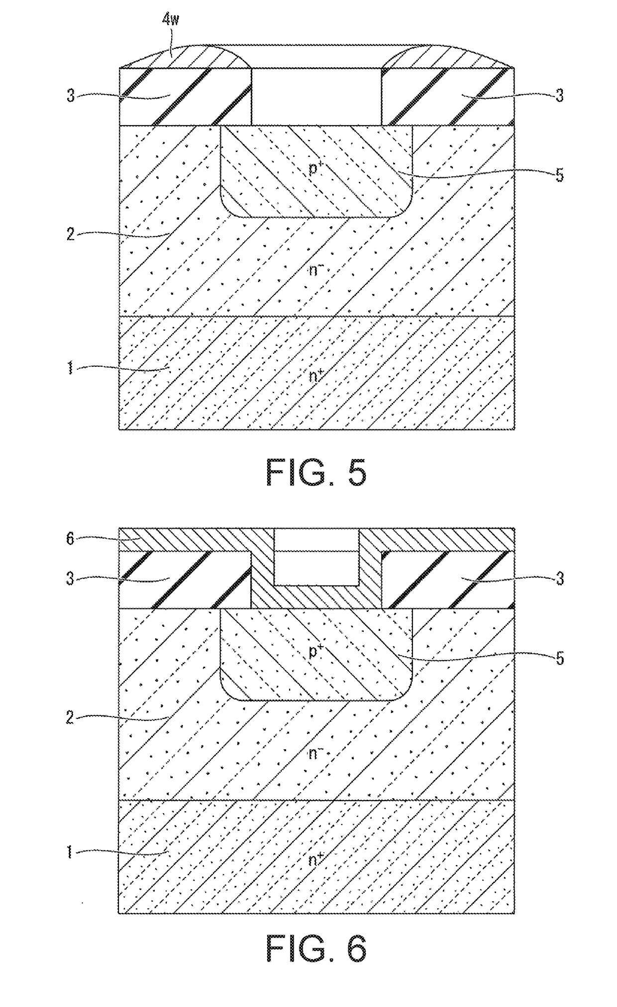
[0054]In a method of manufacturing a semiconductor device according to Embodiment 1, a power p-n diode as illustrated in FIG. 8 is manufactured as an SiC semiconductor device. The semiconductor device illustrated in FIG. 8 includes an n-type (n+) supporting layer (SiC substrate) 1 of a high impurity concentration and an n-type (n) to-be-doped layer 2 of a low impurity concentration formed on the upper surface (the silicon (Si) plane) of the supporting layer 1. A p-type (p+) impurity-doped layer 5 of a high impurity concentration is formed in an upper portion of the to-be-doped layer 2.

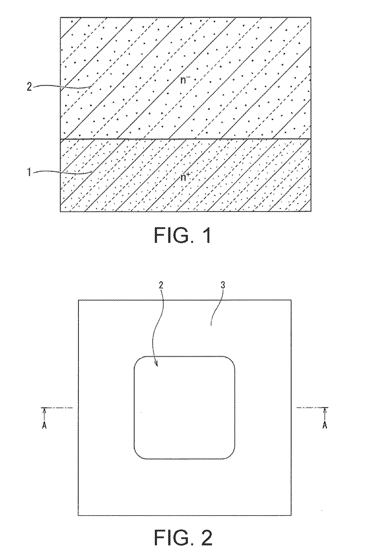
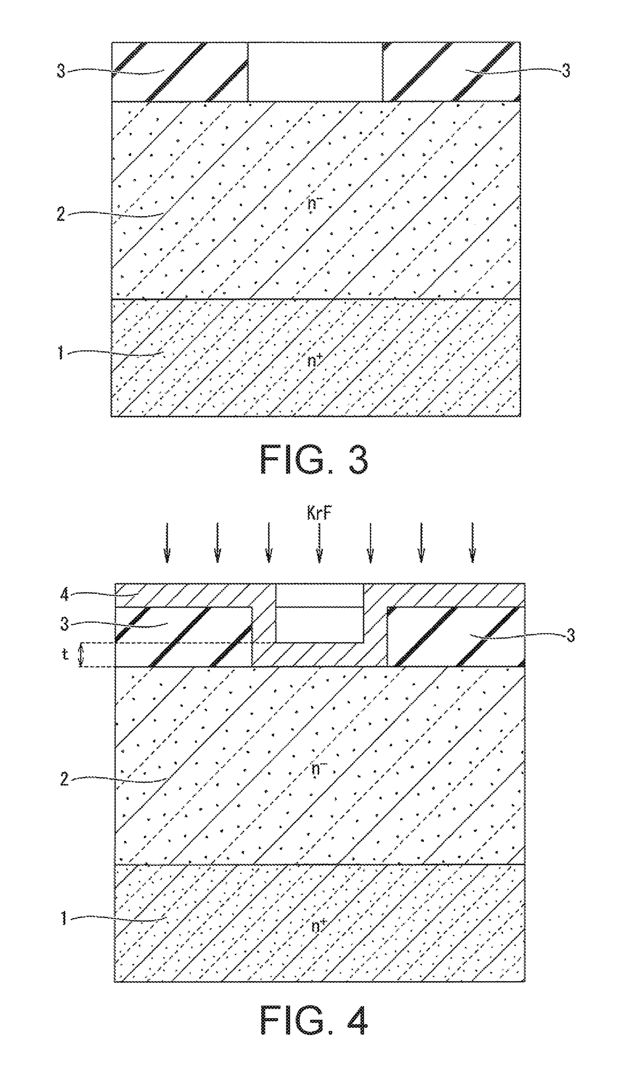
[0055]To manufacture this semiconductor device, first, as illustrated in FIG. 1, a semiconductor substrate (1, 2) including the n+ supporting layer 1 and the n− to-be-doped layer 2 is prepared. The SiC has a monocrystalline 4H crystal structure, and the overall supporting layer 1 has a thickness sufficient to serve as the lower structure of the semiconductor device to be manufactured thereon. When the ...

modification example 1

[0079]As illustrated in FIG. 14, the method of manufacturing a semiconductor device according to Embodiment 1 can be performed by placing the semiconductor substrate (1, 2) inside an airtight chamber 12 and then using a pump 13 or the like to create a vacuum in the chamber 12. Alternatively, the interior of the chamber 12 may be filled with an inert gas atmosphere. The other steps in the method of manufacturing a semiconductor device according to Modification Example 1 are the same as the respective steps described with reference to FIGS. 1 to 8 and therefore will not be described again here.

[0080]In the method of manufacturing a semiconductor device according to Modification Example 1, performing the laser light irradiation process under vacuum or in an inert gas atmosphere makes it possible to reduce the introduction of oxygen into the surface of the semiconductor substrate (1, 2) caused by heat generated during irradiation with laser light. Therefore, in addition to it being poss...

modification example 2

[0081]Moreover, as illustrated in FIG. 15, after forming the second metal film 7 made of Ni or the like on the bottom surface of the semiconductor substrate (1, 2), the contact electrode connected to the n+ supporting layer 1 may be formed by irradiating the second metal film 7 with high-energy laser light instead of by vacuum-annealing at approximately 1000° C. As illustrated in FIG. 16, irradiating the second metal film 7 with laser light promotes silicidation, which makes it possible to form an Ni silicide ohmic contact electrode 7b. The steps other than forming the ohmic contact electrode on the bottom surface side are the same as the respective steps described with reference to FIGS. 1 to 8 and therefore will not be described again here.

[0082]In the method of manufacturing a semiconductor device according to Modification Example 2, instead of performing a high-temperature vacuum-annealing process at approximately 1000° C., a laser light irradiation process is performed to promo...


PUM


Abstract

A method of manufacturing a semiconductor device includes: forming, on a surface of an n-type semiconductor layer, an impurity source film containing both aluminum and beryllium; and forming a p-type impurity-doped layer in the n-type semiconductor layer by irradiating the impurity source film with first laser light to simultaneously introduce the aluminum and the beryllium into the n-type semiconductor layer.

Description

BACKGROUND OF THE INVENTIONTechnical Field[0001]The present invention relates to a method of manufacturing a semiconductor device.Background Art[0002]Semiconductor devices using silicon carbide (SiC) and more particularly 4H silicon carbide (4H-SiC) have attracted attention as power semiconductors. In 4H-SiC semiconductor devices, first, a crystalline layer of 4H-SiC of a desired impurity concentration is epitaxially grown on a high-impurity concentration (impurity density) n+ 4H-SiC semiconductor substrate, for example. Then, impurity elements are introduced into the crystalline layer of 4H-SiC by implanting ions of an n-type impurity element such as phosphorus (P) or a p-type impurity element such as aluminum (Al) or boron (B) into the (0001) plane or the (000-1) plane of the crystalline layer. Forming impurity-doped layers of the desired conductivity types and impurity concentrations within the crystalline layer makes it possible to manufacture a semiconductor device having the d...

Claims


Application Information

Patent Timeline
IPC IPC(8): H01L21/225H01L21/268H01L21/04H01L29/16H01L29/66
CPCH01L21/2254H01L21/268H01L21/046H01L21/0495H01L29/8122H01L29/66053H01L29/7827H01L29/7393H01L29/1608H01L29/45H01L29/6606H01L29/8611H01L29/872H01L29/0619H01L29/66068H01L29/7395H01L29/1095H01L21/0455H01L21/0485H01L21/28512H01L29/7811H01L29/0696
Inventor IGUCHI, KENICHINAKAZAWA, HARUO
Owner FUJI ELECTRIC CO LTD
Why Eureka
Try Eureka