Method for manufacturing laterally insulated-gate bipolar transistor

a technology of lateral insulation and bipolar transistor, which is applied in the field of semiconductor technology, can solve problems affecting product reliability, and achieve the effects of reducing surface electric field, less stress, and significantly reducing the hto wet etching ra

Active Publication Date: 2017-12-14
CSMC TECH FAB2 CO LTD
View PDF0 Cites 2 Cited by
  • Summary
  • Abstract
  • Description
  • Claims
  • Application Information

AI Technical Summary

Benefits of technology

[0006]In the aforementioned method of manufacturing LIGBT, by using HTO, which has a relatively less stress than silicon nitride, as the mini-oxide that reduce the surface electric field of the LIGBT, no dislocation will be introduced on the edge of the active region. By performing a drive-in to the first N well and the first P well, the HTO is densified, the wet etching rate of the HTO is significantly reduced, the etching to the mini-oxide kept from the HTO etching can be stably controlled in the subsequent cleaning process, the stability of volume production is ensured, and the method can thus be applied in volume production.

Problems solved by technology

However, the process has the following defect: as shown in FIG. 1, a large number of dislocations are introduced on the edge of the active region of the device, which will affect the reliability of the product.

Method used


Image

  • Method for manufacturing laterally insulated-gate bipolar transistor
  • Method for manufacturing laterally insulated-gate bipolar transistor
  • Method for manufacturing laterally insulated-gate bipolar transistor

Examples


Embodiment Construction

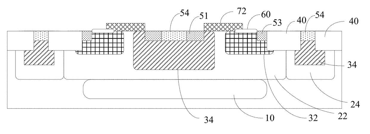
[0012]The present disclosure will be described in the following with reference to the accompanying drawings and the embodiments in order to make the above objects, features and advantages of the present disclosure more apparent, the specific embodiments will be described in detail in combination with the accompanying drawings. Numerous specific details are described hereinafter in order to facilitate a thorough understanding of the present disclosure. The various embodiments of the disclosure may, however, be embodied in many different forms and should not be construed as limited to the specific embodiments set forth hereinafter, and people skilled in the art can make similar modifications without departing from the spirit of the present disclosure.

[0013]It should be understood that when an element is defined as “fixed to” another element, it is either directly on an element or indirectly on an element with a mediating element. When an element is considered being “connected” to anot...


PUM


Abstract

The present invention relates to a method for manufacturing a laterally insulated-gate bipolar transistor, comprising: providing a wafer having an N-type buried layer (10), an STI (40), and a first N well (22)/a first P well (24) which are formed successively from above a substrate; depositing and forming a high-temperature oxide film on the first N well (22) of the wafer; performing thermal drive-in on the wafer and performing photoetching and etching on the high-temperature oxide film to form a mini oxide layer (60); performing photoetching and ion implantation so as to form a second N well (32) inside the first N well (22) and second P wells (34) inside the first N well (22) and the first P well (24); then successively forming a gate oxide layer and a polysilicon gate (72), wherein one end of the gate oxide layer and the polysilicon gate (72) extends onto the second P well (34) inside the first N well (22), and the other end extends onto the mini oxide layer (60) on the second N well (32); and photoetching and injecting N-type ions between the mini oxide layer (60) and the STI (40) adjacent to the mini oxide layer (60) to form a drain electrode, and at the same time forming a source electrode (51) inside the second P well (34).

Description

FIELD OF THE INVENTION[0001]The present disclosure relates to the semiconductor technology, and in particular relates a method of manufacturing the lateral insulated-gate bipolar transistor (LIGBT).BACKGROUND OF THE INVENTION[0002]As for a BIPOLAR-CMOS-DMOS (BCD) platform of 0.18 micrometers, after adding a mini-oxide structure of silicon dioxide material on a side of the channel region that is adjacent to the drain, the surface electric field of the LDMOS can be significantly reduced without increasing the region of the LDMOS, thereby addressing the degradation problem of the Idlin (linear drain current) / Rdson (on resistance) after a current and voltage test.[0003]As to this mini-oxide, the conventional process utilizes silicon nitride as a hard mask to grow silicon dioxide via furnace tube and in certain region (i.e. the Local Oxidation of Silicon (LOCOS) technology). In particular, the silicon nitride can be used as a hard mask, a region that is required to have mini-oxide formed...

Claims


Application Information

Patent Timeline
Patent Type & Authority Applications(United States)
IPC IPC(8): H01L29/66H01L29/40H01L21/311H01L29/739H01L29/06H01L21/02H01L21/265
CPCH01L29/66325H01L21/02318H01L29/408H01L21/02271H01L21/26513H01L29/7393H01L21/02164H01L29/0653H01L21/02211H01L21/31116H01L29/78
Inventor HUANG, FENGHAN, GUANGTAOSUN, GUIPENGLIN, FENGZHAO, LONGJIELIN, HUATANGZHAO, BINGLIU, LIXIANGPING, LIANGLIANGCHEN, FENGYING
Owner CSMC TECH FAB2 CO LTD
Why Eureka
Try Eureka