
Device for switching a semiconductor-based switch and sensor for detecting a current change velocity at a semiconductor-based switch

Inactive Publication Date: 2017-04-13
FRAUNHOFER GESELLSCHAFT ZUR FOERDERUNG DER ANGEWANDTEN FORSCHUNG EV
View PDF3 Cites 5 Cited by
  • Summary
  • Abstract
  • Description
  • Claims
  • Application Information

AI Technical Summary

Benefits of technology

The patent describes a device that can control a semiconductor-based switch by applying multiple voltage and resistance values to its control terminal. This allows for precise control of the switch, and the transmission path can be changed dynamically for even better control. The device also recycling charge carriers to improve efficiency and reduce switching losses. Additionally, it provides a contactless detection system to accurately detect the current change velocity of the power current flowing through the switch. The insulating foil used for detection ensures high voltage safety, and the detection is very accurate. The sensor's measurement voltage can also be adjusted easily. These three aspects can be combined to achieve further advancement in the field.

Problems solved by technology

It is a disadvantage of such an implementation that the driving power is not optimal for each switching time / operating time, that the switching losses can only be optimized for one operating point (voltage, load current, temperature).
Further, a tradeoff has to be found between short death / delay time and di / dt behavior, du / dt behavior as well as power losses in the tail phase.
Further, it is disadvantageous that the switching sequence does not compensate any component leakages, that high effort is necessitated when using new or different power switches for changing the topology or for adapting the switching behavior by component changes, that no flexible adaptation or scalability is given as well as no high or no configurable degree of protection is possible.
Interference radiation conforming to standard heavily influences the losses and is not suitable for a partial load at the switch 12.
Disadvantages of such an embodiment are an increased need for components, a more complex sequence control as well as additional (galvanically isolated) control channels.
This results in increased costs.
Further, it is disadvantageous that switching losses can be optimized only for one operating point (voltage, load current, temperature), that the switching sequence does not compensate any component leakages, that high effort results when using new / different power switches, that no flexible adaptation / scalability of the circuit is possible, that no high or even configurable degree of protection can be obtained.
Further, interference radiation conforming to standards can be obtained, which influences the switching losses to a lesser degree.
It is a disadvantage that increased need for components, more complex sequence control as well as additional (galvanically isolated) control channels result which result in increased costs.
Switching losses can only be optimized for one operating point (voltage, load current, temperature).
Further, the switching sequence does not compensate any component leakages.
A high effort results when using new / different power switches, no flexible adaptation / scalability of the system is possible, and no high or even configurable degree of protection can be obtained.
Implementing a second voltage level causes additional losses, depending on the realization.
The disadvantages of this concept are that a significantly increased need for components results, mostly expensive analog components having a high bandwidth are necessitated, increased losses occur in the GDU by components having a high bandwidth, that feedback circuits cause additional losses due to intervention, that increased costs occur, that switching losses can only be optimized for one operating point (voltage, load current, temperature), that the switching sequence does not compensate any component leakages, that high effort results when using new / different power switches, that no flexible adaptation or scalability of the concept is possible, that merely a configurable but no high degree of protection can be obtained, that a high voltage potential (collector) necessitates installation space on a driver area, since air and creeping distances have to be considered, that high voltage components have great leakages, that no adaptation of the control plane is possible by interventions of the feedbacks, that the usage of the measured parasitic leakage inductance of the power switch is no precisely specified characteristic of the power switch itself, that with small leakage inductances no direct processing of the signal is possible and that the direct intervention with feedback comprises a phase shift such that the intervention, depending on the impedances in the gate line, only has a limited or no effect in fast switching processes and can result in undesirable oscillations.
The disadvantages of this concept are a significantly increased need for components due to two programmable instances, that mostly expensive analog components having a high bandwidth are necessitated, that increased losses occur in the GDU due to two programmable instances, that increased costs can result when using high-performance DSP and / or FPGA, that no optimization of the actual switching edge curve is necessitated preferential direction / possible, that switching losses can only be optimized for one operating point (voltage, load current, temperature), that the switching sequence does not compensate any component leakages, that a high effort results when using new / different power switches, that no flexible adaptation / scalability is possible and that merely a configurable but no high degree of protection can be obtained.
However, it is a disadvantage of this concept that a significantly increased need for components results by a total of 14 switching paths, wherein also significantly increased costs result by 14 switching paths.
The concept has poor efficiency as never all paths are used at any time.
Further, great space requirements result due to a plurality of control paths and feedback paths.
The usage of the parasitic leakage inductance of the power switch is no specifically specified characteristic of the power switch resulting in measurement inaccuracies.
The usage of high-performance DSP and FPGA results in increased costs when implementing the concept.
Further, the switching sequence does not compensate any component leakage.
Here, the main problem is the delay due to the signal processing times. Thus, directly intervening into the dynamic switching behavior is only possible with very slow edge curves.
In summary, the main problem of all controlled methods, independent of whether the same are analog or digital is the lack of adaptation to the operating point of the power unit.
Some component leakages and parameter variances of the power switches cannot be compensated.
All analog-controlled methods have the problem, as long as they have direct influence on the current switching edge, that they necessitate very expensive energy-hungry components having a high bandwidth resulting in a low energy efficiency.
Thus, additional control losses are generated.
Since the leakage inductance is generally very small and continuously optimized, no direct processing can be performed.
The same are mostly expensive and frequently too inaccurate for signal processing since the same are not operated in the optimum operating point.
Apart from that, looping-in this potential results in a large unused installation area due to the necessitated voltage clearances.
The problem of known digitally controlled solutions is also the lack of independent adaptation to the current operating point or the component leakage.
Unused paths represent unused areas and still cause component costs since the same are populated.

Method used


Image

  • Device for switching a semiconductor-based switch and sensor for detecting a current change velocity at a semiconductor-based switch
  • Device for switching a semiconductor-based switch and sensor for detecting a current change velocity at a semiconductor-based switch
  • Device for switching a semiconductor-based switch and sensor for detecting a current change velocity at a semiconductor-based switch

Examples


Embodiment Construction

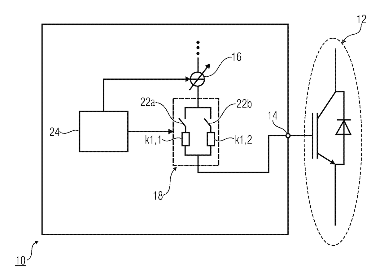
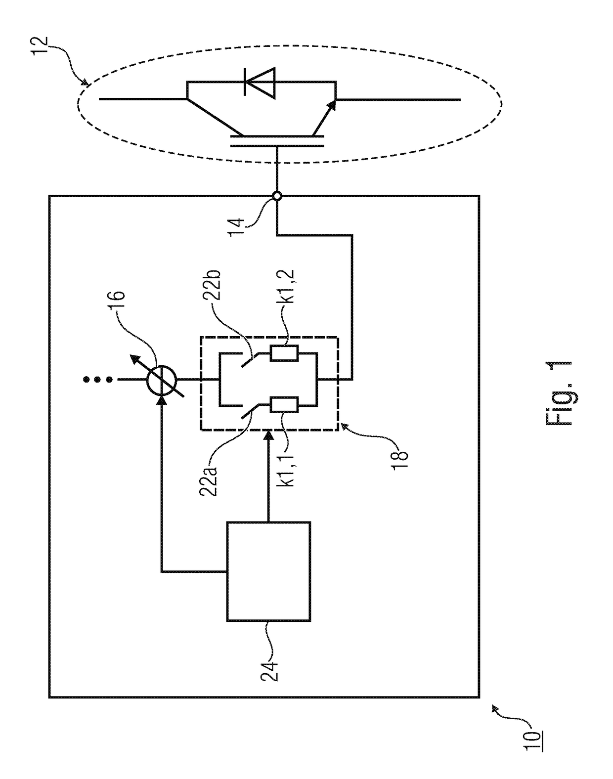
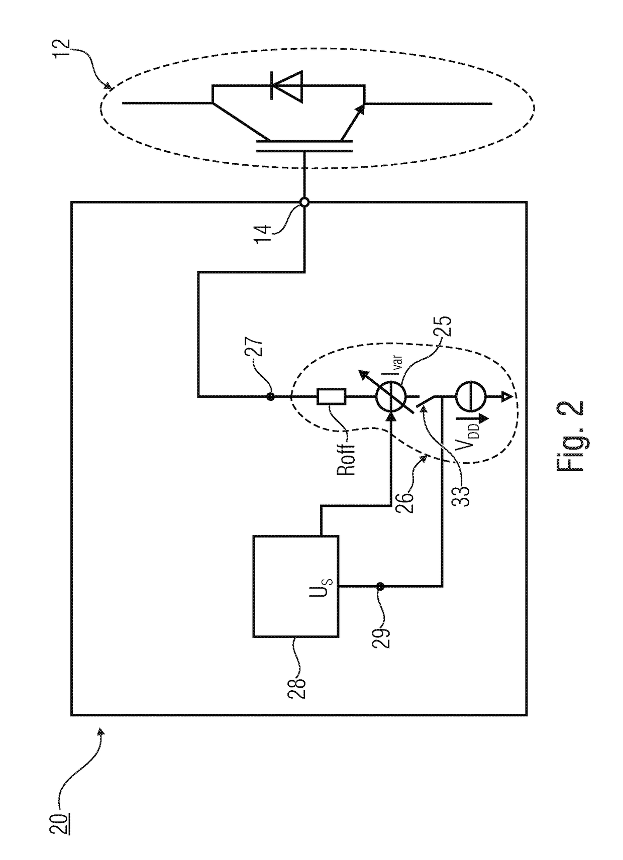
[0061]Before embodiments of the present invention will be discussed in more detail below based on the drawings, it should be noted that identical, functionally equal or equal elements, objects and / or structures in the different figures are provided with the same reference numbers, such that the description of these elements illustrated in the different embodiments is inter-exchangeable or inter-applicable.

[0062]Embodiments describe below relate to switching a semiconductor-based switch, such as a metal oxide semiconductor field effect transistor (MOSFET) or an insulated gate bipolar transistor (IGBT).

[0063]The semiconductor-based switch can be of an n channel or p channel type. Further, the semiconductor-based switch can have a normally conductive or normally non-conductive configuration. Based on a concentration of charge carriers stored on a control capacitance (gate capacitance) connected to the control terminal of the semiconductor-based switch (gate terminal), a switch state, f...


PUM


Abstract

A device for switching a semiconductor-based switch includes a terminal that is configured to be connected to a control terminal of the semiconductor-based switch. A controllable deactivation voltage source connected to the terminal is configured to provide, at least temporarily, a switching potential at a potential node. A control device is configured to control the controllable deactivation voltage source in a time-varying manner, such that the controllable deactivation voltage source provides the switching potential at the potential node during a switching interval. The switching potential is galvanically coupled to a supply node to which a supply potential of the control device is applied and has a lower potential value than a threshold voltage of the semiconductor-based switch. The control device is configured to control the controllable deactivation voltage source.

Description

CROSS-REFERENCE TO RELATED APPLICATIONS[0001]This application is a continuation of copending International Application No. PCT / EP2015 / 058189, filed Apr. 15, 2015, which is incorporated herein by reference in its entirety, and additionally claims priority from European Application No. EP 14165895.5, filed Apr. 24, 2014, and German Application No. 102014214260.1, filed Jul. 22, 2014, which are all incorporated herein by reference in their entirety.[0002]The present invention relates to devices for switching a semiconductor-based switch and to a sensor for detecting a current change velocity of a power current flowing through a semiconductor-based switch.BACKGROUND OF THE INVENTION[0003]Nowadays, so-called power converters are used for converting electric energy. The same allow the connection of energy sources with given voltages, currents and frequencies to energy sinks or loads. Here, the converter converts electric energy of one form, such as alternating current (AC), direct current...

Claims


Application Information

Patent Timeline
Patent Type & Authority Applications(United States)
IPC IPC(8): H02J4/00G01R15/18
CPCG01R15/18H02J4/00H01L23/62H01L2924/0002H03K2217/0027H03K17/0828H03K17/165H03K17/168G01R19/12H03K17/0822H03K17/166H02M1/08G01R15/183H02M1/0009H01L2924/00G01R19/14
Inventor HOPPERDIETZEL, RENE
Owner FRAUNHOFER GESELLSCHAFT ZUR FOERDERUNG DER ANGEWANDTEN FORSCHUNG EV
Learn More