Aqueous composition for etching of copper and copper alloys
a technology of etching composition and copper alloy, which is applied in the direction of electrical equipment, decorative surface effects, decorative arts, etc., can solve the problems of inability to use conventional etching solutions, disadvantages of known etching solutions, and on-going miniaturization of circuits in terms of line width, value and thickness of copper layers to be etched, so as to minimize the risk of circuit shorts between individual copper or copper alloy structures
- Summary
- Abstract
- Description
- Claims
- Application Information
AI Technical Summary
Benefits of technology
Problems solved by technology
Method used
Image
Examples
example 1
Comparative
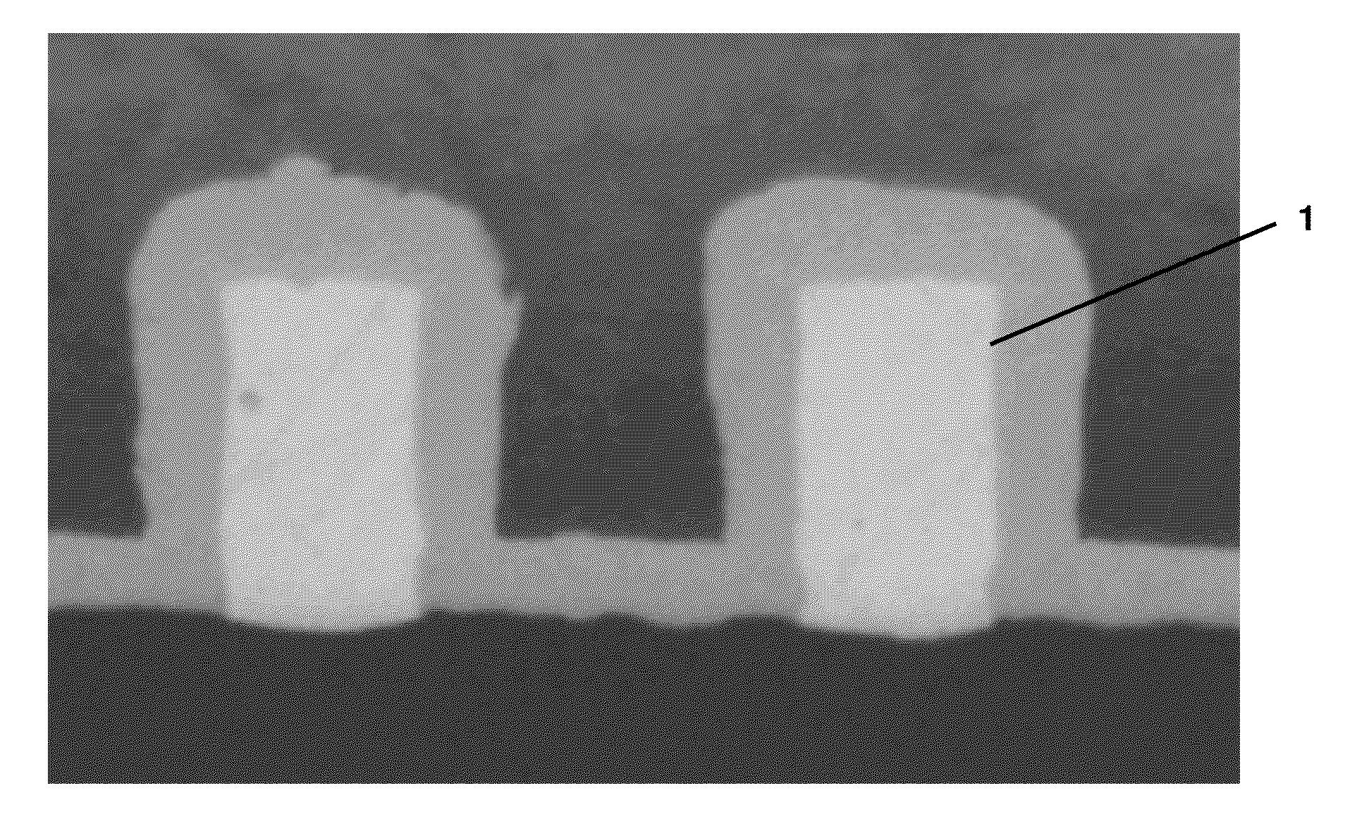
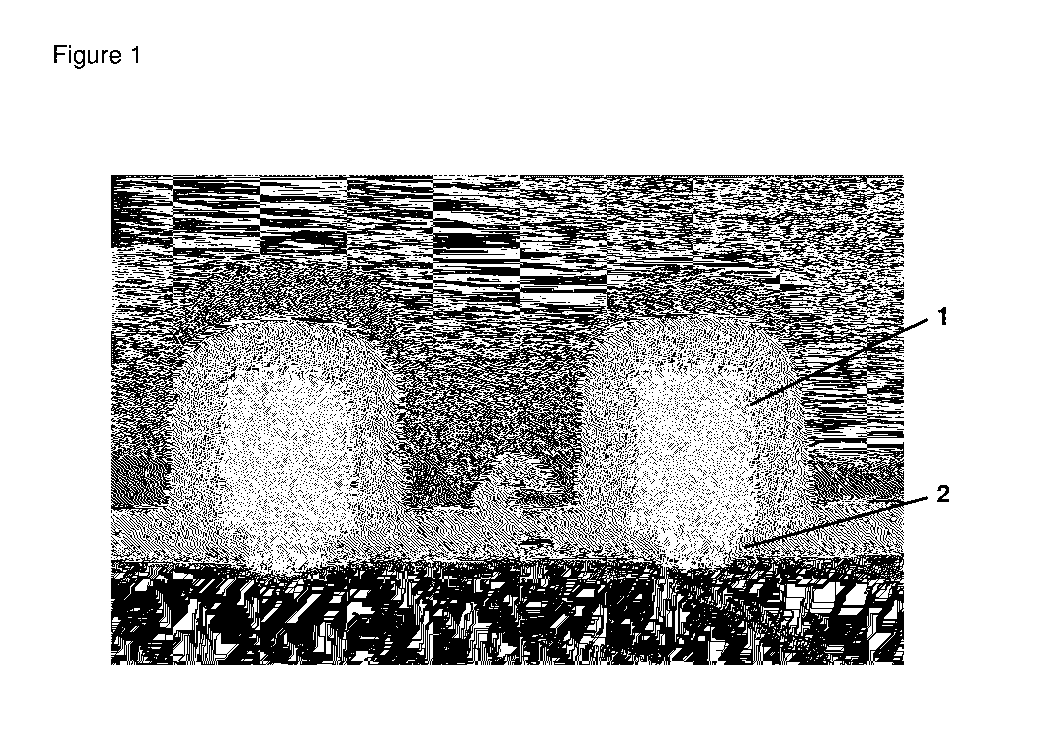
[0067]An aqueous composition consisting of 20 g / l H2O2 and 90 g / l sulfuric acid was applied as etching solution.
[0068]The resulting line shape of copper tracks (track width: 8 μm, track height: 10 μm) is shown in FIG. 1. The copper tracks 1 show a severe undercutting 2 of the track base (i.e. the seed layer obtained by electroless plating of copper). Hence, the copper track has not the required rectangular shape and no sufficient adhesion to the underlying dielectric substrate.
example 2
Comparative
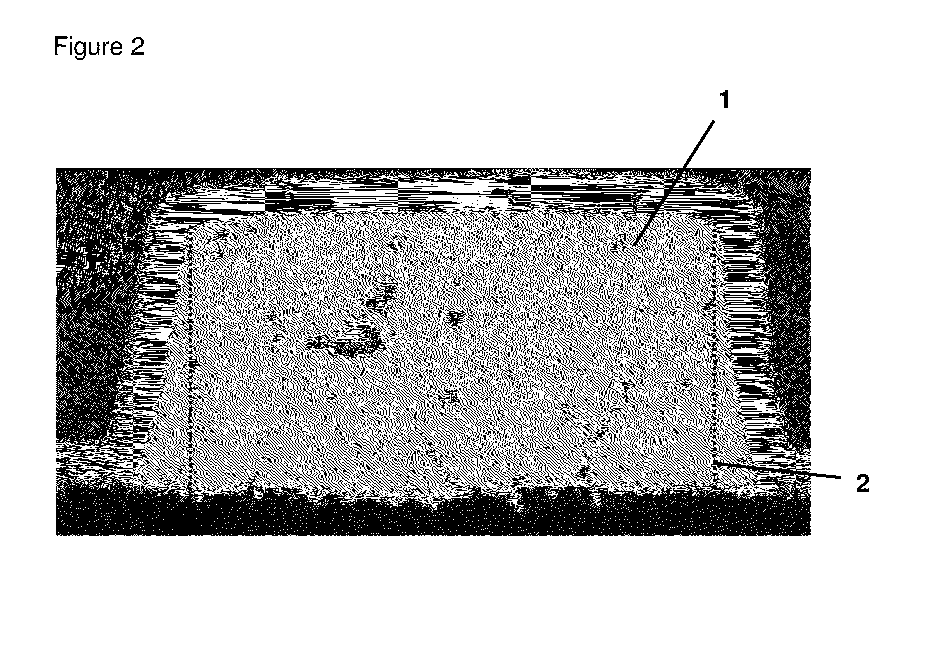
[0069]An aqueous composition consisting of 5 g / l Fe2(SO4)3 and 90 g / l sulfuric acid was applied as etching solution.
[0070]The resulting line shape of the copper tracks (track width: 20 μm, track height: 10 μm) is shown in FIG. 2. The copper track 1 shows a strong trapezoidal shape indicated by the dotted lines 3. Hence, the copper track does not provide the desired rectangular shape and poses the danger of circuit shorts or cross-talk between individual tracks.
example 3
[0071]An aqueous composition consisting of 15 g / l Fe2(SO4)3, 90 g / l sulfuric acid, 15 mg / l benzotriazole, and 0.7 g / l of an etching additive according to formula (I) wherein R1 is H, R2 is Na+ and R3 is 2-ethyl-hexyl was applied as etching solution.
[0072]The resulting line shape of the copper tracks (track width: 8 μm, track height: 10 μm) is shown in FIG. 3. The copper tracks 1 have the desired rectangular line shape, have a sufficient adhesion to the underlying dielectric substrate and pose no risk for circuit shorts or cross-talk between individual tracks.
PUM
| Property | Measurement | Unit |
|---|---|---|
| concentration | aaaaa | aaaaa |
| concentration | aaaaa | aaaaa |
| concentration | aaaaa | aaaaa |
Abstract
Description
Claims
Application Information
 - R&D
- Intellectual Property
- Life Sciences
- Materials
- Tech Scout
- Unparalleled Data Quality
- Higher Quality Content
- 60% Fewer Hallucinations
Browse by: Latest US Patents, China's latest patents, Technical Efficacy Thesaurus, Application Domain, Technology Topic, Popular Technical Reports.
© 2025 PatSnap. All rights reserved.Legal|Privacy policy|Modern Slavery Act Transparency Statement|Sitemap|About US| Contact US: help@patsnap.com


