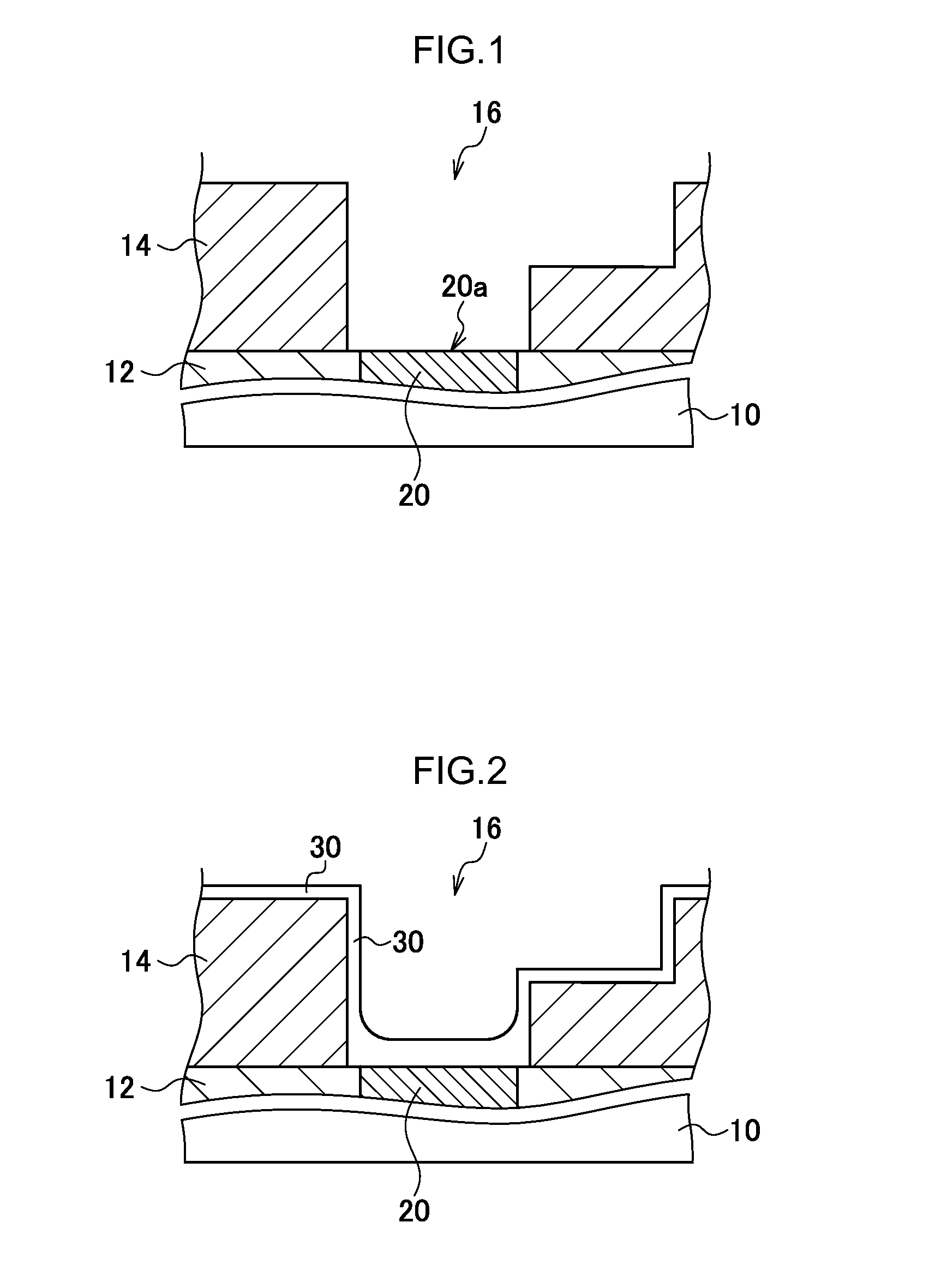
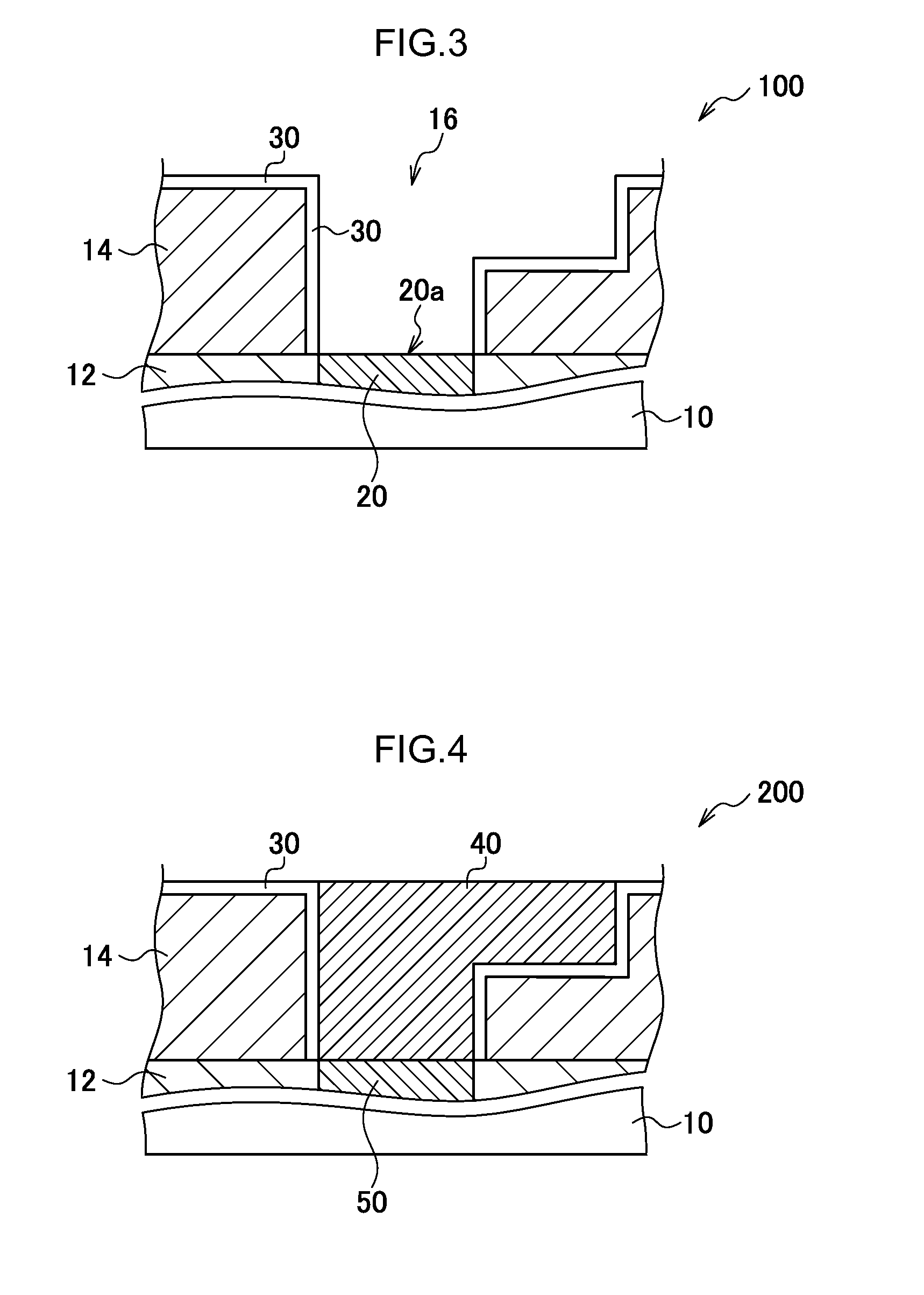
Semiconductor device, method for manufacturing the same, and rinsing liquid
a technology of semiconductors and liquids, applied in the direction of coatings, basic electric elements, chemistry apparatus and processes, etc., can solve the problems of increasing the dielectric constant or occurrence of current leakage in some cases, etc., to improve the interconnection resistance of the connection portion, and improve the plasma resistance of the sealing layer.
- Summary
- Abstract
- Description
- Claims
- Application Information
AI Technical Summary
Benefits of technology
Problems solved by technology
Method used
Image


Examples
example 1
[0370]>
[0371]
[0372]77.4 g of bis(triethoxysilyl)ethane and 70.9 g of ethanol were mixed and stirred at room temperature, and then 80 mL of 1 mol / L nitric acid were added thereto, and the resultant was stirred at 50° C. for 1 hour. Subsequently, a solution obtained by dissolving 20.9 g of polyoxyethylene (20) stearyl ether in 280 g of ethanol was dropwise added thereto and mixed. After mixing, the mixture was stirred at 30° C. for 4 hours. The resulting solution was concentrated to 105 g at 25° C., under a reduced pressure of 30 hPa. After concentration, a solution obtained by mixing 1-propyl alcohol and 2-butyl alcohol at a volume ratio of 2:1 was added thereto, to obtain a precursor solution in an amount of 1,800 g.
[0373]
[0374]3.4 g of dimethyldiethoxysilane and 1.8 g of hexamethyldisiloxane were added to 472 g of the precursor solution, and the mixture was stirred at 25° C. for 1 hour, to obtain a composition for forming porous silica. In the addition, the amount of dimethyldietho...
examples 2 and 3
[0441]Evaluations were conducted in the same manner as that in Example 1, except that the pressure in the heat treatment was changed as noted in Table 1 below.
[0442]The results of the evaluations are indicated in Table 1 below.
example 4
[0443]Evaluations were conducted in the same manner as that in Example 1, except that the method of forming a sealing layer was changed as described below, and that the washing as described below was carried out between the formation of the sealing layer and the heat treatment.
[0444]The results of the evaluations are indicated in Table 1 below.
[0445]
[0446]The procedures “C” as defined in Example 1 were carried out with respect to the substrate (the silicon wafer provided with the low-k film, the silicon wafer, or the copper substrate). Thereafter, the substrate was placed on a hotplate, and thermally treated at 125° C. for 60 seconds in the atmospheric air. In this way, a sealing layer was formed on the substrate.
[0447]The above procedures for forming a sealing layer are represented by “C→B” in Table 1 below.
[0448]
[0449]While the substrate, on which a sealing layer had been formed as described above, was rotated at 600 rpm using a spin coater, ultrapure water as a rinsing liquid (ha...
PUM
| Property | Measurement | Unit |
|---|---|---|
| temperature | aaaaa | aaaaa |
| temperature | aaaaa | aaaaa |
| temperature | aaaaa | aaaaa |
Abstract
Description
Claims
Application Information
 - R&D
- Intellectual Property
- Life Sciences
- Materials
- Tech Scout
- Unparalleled Data Quality
- Higher Quality Content
- 60% Fewer Hallucinations
Browse by: Latest US Patents, China's latest patents, Technical Efficacy Thesaurus, Application Domain, Technology Topic, Popular Technical Reports.
© 2025 PatSnap. All rights reserved.Legal|Privacy policy|Modern Slavery Act Transparency Statement|Sitemap|About US| Contact US: help@patsnap.com