Electromagnetic induction sensor, overlay member for electromagnetic induction sensor, and manufacturing method of electromagnetic induction sensor
a manufacturing method and technology of electromagnetic induction sensor, applied in the direction of instruments, liquid/fluent solid measurement, conductive pattern formation, etc., can solve the problems of large characteristic variation, difficult cutting of amorphous alloy, etc., to achieve easy stamping, easy cutting, and low hardness
- Summary
- Abstract
- Description
- Claims
- Application Information
AI Technical Summary
Benefits of technology
Problems solved by technology
Method used
Image
Examples
first embodiment
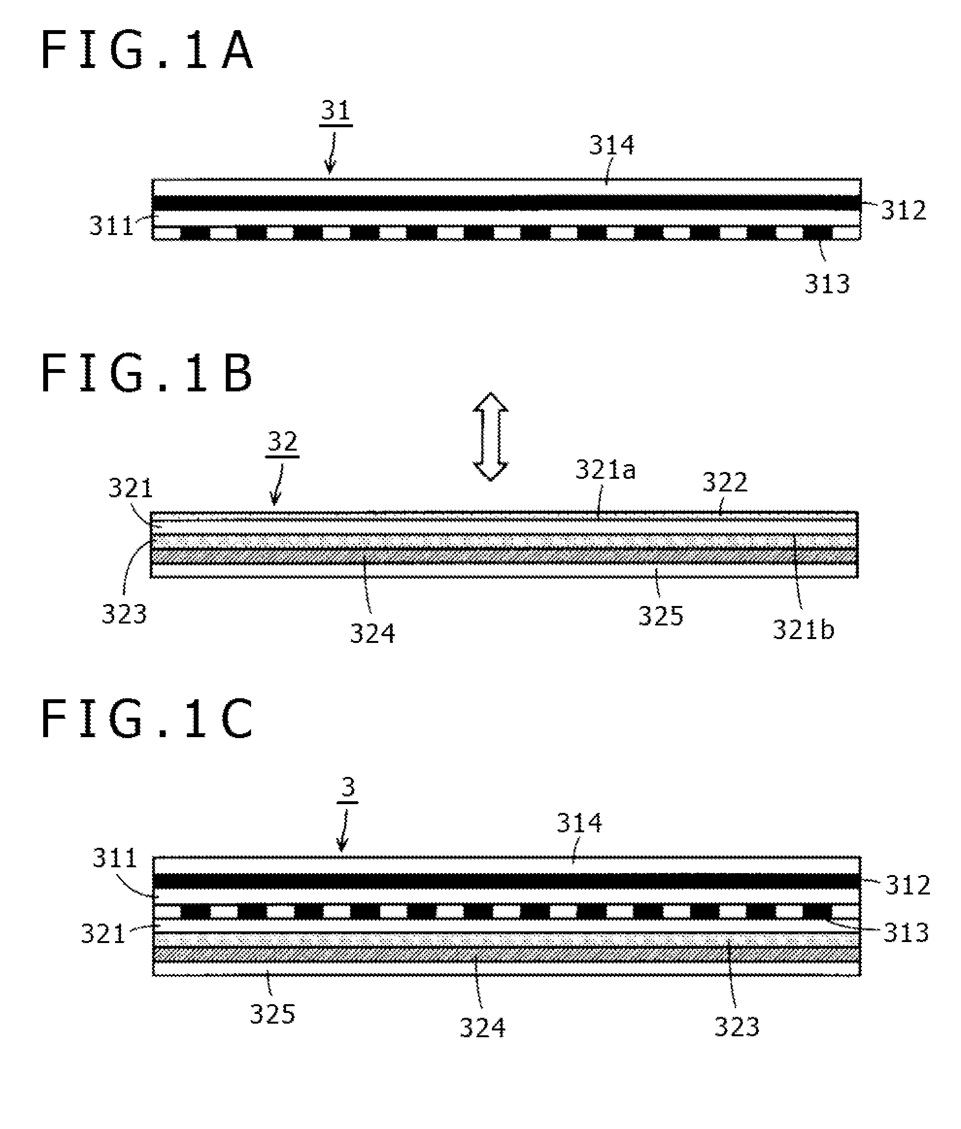
[0043]FIGS. 1A to 1C are sectional views showing a configuration example of an electromagnetic induction sensor according to a first embodiment of the invention. An electromagnetic induction sensor 3 of the first embodiment is composed of a sensor board main body 31 shown in FIG. 1A and an overlay member 32 shown in FIG. 1B. The sensor 3 is integrally formed by depositing (adhering) the overlay member 32 on (to) the sensor board main body 31 (see FIG. 1C).
[0044]As shown in FIG. 1A, in the sensor board main body 31, an X-axis-direction loop coil group conductor 312 is disposed on one surface side of an insulating substrate 311 composed of, for example, PET and a Y-axis-direction loop coil group conductor 313 is disposed on the other surface side opposite from the one surface. Furthermore, in the example of FIG. 1A, a surface sheet (overlay) 314 formed of, for example, a PET film is so deposited (adhered) as to cover the X-axis-direction loop coil group conductor 312 as a whole. A pos...
second embodiment
[0104]In the above-described first embodiment, with respect to the Y-axis-direction loop coil group conductor 313 of the sensor board main body 31, the magnetic powder material layer 323 is deposited (adhered / applied) with the intermediary of an insulating layer formed of the overlay base film 321. However, because the magnetic powder material layer 323 has resistance as high as 100 kΩ as shown in the table of FIG. 5, even when the insulating layer formed of the overlay base film 321 is not provided, there may be practically no influence on the electrical characteristics of the Y-axis-direction loop coil group conductor 313. Thus, the overlay base film 321 may be omitted. By employing the configuration in which the insulating layer formed of the overlay base film 321 is not provided, a sensor can be realized whose thickness is even smaller than that of the sensor 3 of the first embodiment.
[0105]The second embodiment provides an electromagnetic induction sensor having such configurat...
other embodiments and modification examples
[0126]In the explanation of the above-described embodiments, a material made into a coating material form or a material impregnated with an adhesive is used as the magnetic powder material. However, the magnetic powder material may be provided as a material obtained by mixing powder of a high-permeability amorphous metal or the like with a non-magnetic, non-conductive polymer material, such as resin, and solidifying the mixture. It should be apparent to those skilled in the art that the above-described stamping processing can be similarly performed in this case.
[0127]Although the number of processing steps is reduced in the above-described stamping processing, it should be apparent to those skilled in the art that the electromagnetic induction sensor of an embodiment of the present invention may be produced similarly to the related art. For example, a manufacturing method may be used, in which the overlay member 32 is subjected to outer shape processing (cut) in advance and the over...
PUM
| Property | Measurement | Unit |
|---|---|---|
| thickness | aaaaa | aaaaa |
| thickness | aaaaa | aaaaa |
| thickness | aaaaa | aaaaa |
Abstract
Description
Claims
Application Information
 - R&D
- Intellectual Property
- Life Sciences
- Materials
- Tech Scout
- Unparalleled Data Quality
- Higher Quality Content
- 60% Fewer Hallucinations
Browse by: Latest US Patents, China's latest patents, Technical Efficacy Thesaurus, Application Domain, Technology Topic, Popular Technical Reports.
© 2025 PatSnap. All rights reserved.Legal|Privacy policy|Modern Slavery Act Transparency Statement|Sitemap|About US| Contact US: help@patsnap.com


