Laser processing apparatus and laser processing method

Inactive Publication Date: 2015-01-15
AISIN SEIKI KK +1
View PDF8 Cites 3 Cited by
  • Summary
  • Abstract
  • Description
  • Claims
  • Application Information

AI Technical Summary

Benefits of technology

The invention offers a laser processing apparatus and method that can go deeper into the substrate surface and speed up processing while minimizing damage to the surface. This allows for more effective and efficient use of laser processing techniques.

Problems solved by technology

This is because where the pulse width is too short, the peak intensity becomes too large and the thermal effect time is too short, and where the pulse width is too long, the peak intensity decreases.
This is because the absorption coefficient of amorphous silicon as a processing object is not too small, and where the wavelength becomes too long, it is not desirable in view of efficient heating of the processing object.
However, where the laser beam spot is decreased in size, the surface area of annealing performed by multi-photon absorption also decreases.
Therefore, in the annealing using a femtosecond laser, it is difficult to control the processing state and select the processing conditions.
In this case, where dirt or defects are present on the substrate surface, absorption edges appear that are caused thereby and unintentional ablation processing can be performed.
Therefore, for example, where the annealing is performed by scanning a laser beam in a certain direction on a substrate, linear processing is performed on the substrate following this scanning, which results in a damaged substrate surface.
The thermal diffusion length with a femtosecond laser beam is less than that with a nanosecond laser beam, and heat transfer is more difficult with the femtosecond beam.
In this case, the substrate surface may be thermally damaged by heating with the high-intensity laser beam.
In the explanation above, amorphous silicon is considered by way of example as a material to be annealed, but in laser annealing using a nanosecond laser beam, the annealing reaching deep portions from the substrate is difficult to perform.

Method used


Image

  • Laser processing apparatus and laser processing method
  • Laser processing apparatus and laser processing method
  • Laser processing apparatus and laser processing method

Examples


first embodiment

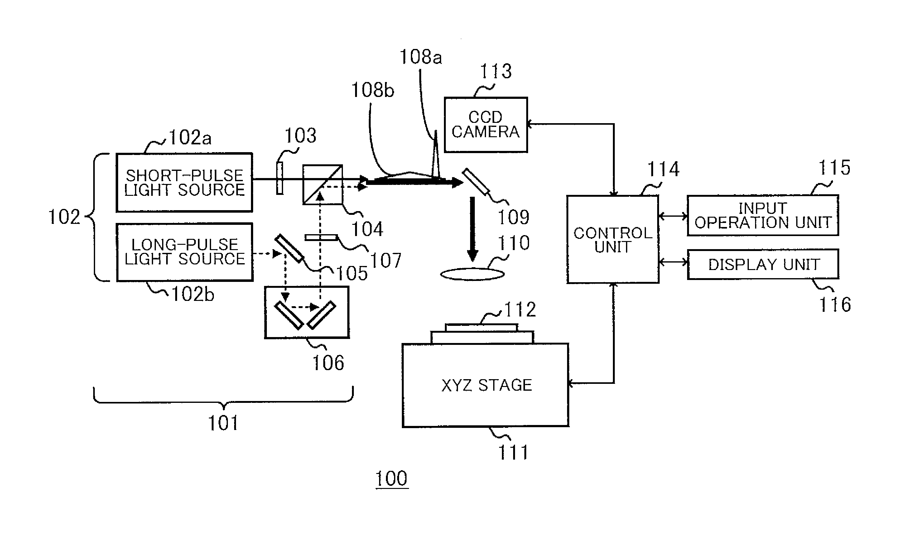
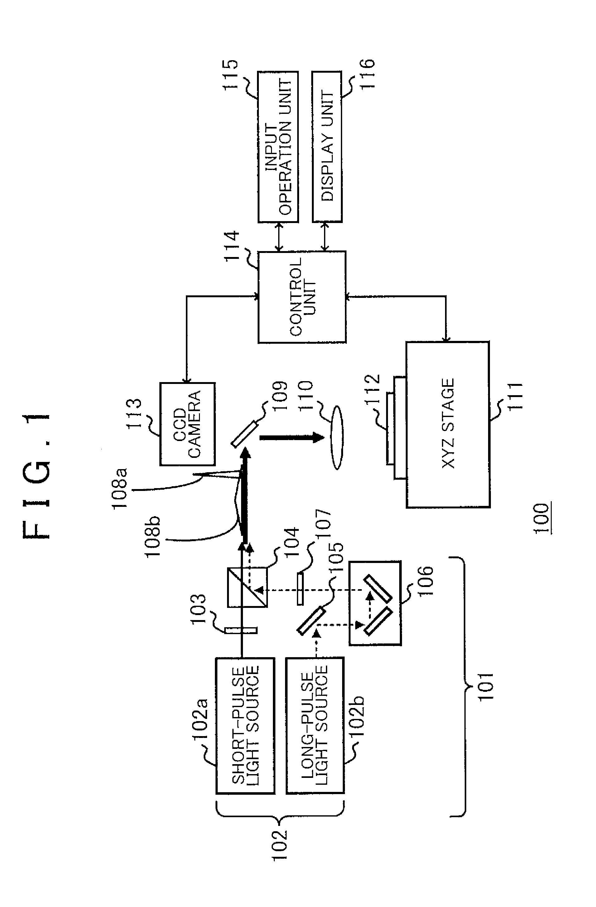
[0024]In the present embodiment, a first pulse laser beam and a second pulse laser beam are used, a starting point region serving as a starting point for forming a high-temperature portion is formed by the first pulse laser beam in the predetermined region (surface of a preprocessing object, for example, a semiconductor layer such as a silicon layer, or inside the processing object) of the processing object, and then the starting point region is heated with the second pulse laser beam to raise the temperature of a region (high-temperature portion) including the starting point region. Annealing such as crystallization and activation is an example of such heating treatment. The above heating treatment can be also used for local heating treatment other than the annealing.

[0025]More specifically, a region (can be also referred to hereinbelow as “light absorptance increase region”) with a light absorptance higher than that in other regions of the processing object is temporarily formed o...

examples

[0075]A phosphorus-doped Si substrate was used as the processing object 112, and the Si substrate was laser annealed according to the present embodiment.

[0076]In the first and second examples, a femtosecond laser beam with a wavelength of 1050 nm, a repetition frequency of 1 MHz, and a pulse width of 800 fs was used as the first pulse laser beam, and a nanosecond laser beam with a wavelength of 1050 nm, a repetition frequency of 1 MHz, and a pulse width of 10 ns was used as the second pulse laser beam. The power of the femtosecond laser beam and nanosecond laser beam was set to the values shown in Table 1. The femtosecond laser beam and nanosecond laser beam had a spot diameter of 130 μm, and the scanning rate of the XYZ stage 111 was 600 mm / s. The time interval between the femtosecond laser beam and nanosecond laser beam was 3 ns. In the present examples, the region of the Si substrate, which was the processing object 112, at a depth of about 1 μm was doped with phosphorus. Accordi...

second embodiment

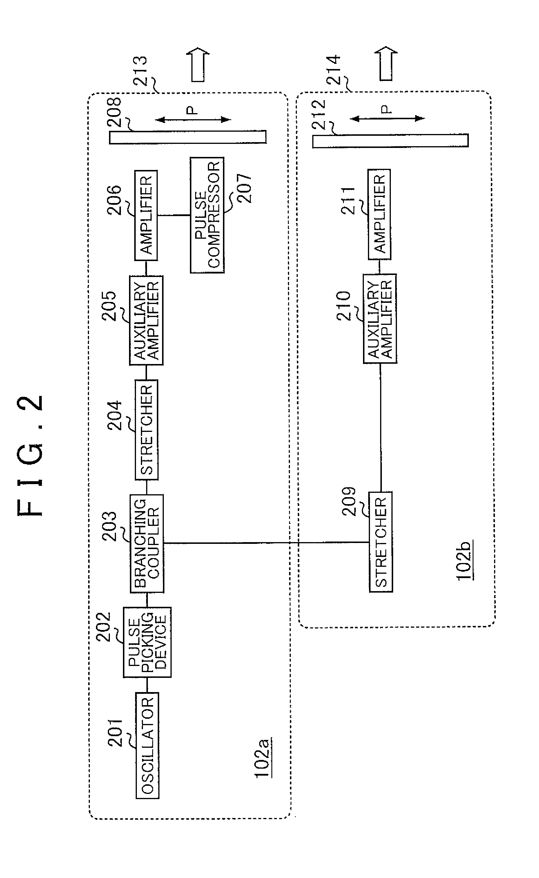
[0081]In the present embodiment, the beam spot diameter and laser beam focus point position of the first pulse laser beam (for example, femtosecond laser beam) and the second pulse laser beam (for example, nanosecond laser beam) are preferably set such that: (1) the conditions (energy density, pulse width, etc.) at which the first pulse laser beam generates multi-photon absorption and induces plasma (light absorptance increase region) are fulfilled, and (2) the second pulse laser beam is absorbed by the plasma (light absorptance increase region) generated by the first pulse laser beam.

[0082]Considered below is the case in which a femtosecond laser beam is used as the first pulse laser beam and a nanosecond laser beam is used as the second pulse laser beam. Plasma generated by the femtosecond laser beam is generated close to the focus point. The plasma is not generated where the energy density is not equal to or higher than a predetermined value. Therefore, the plasma size is apparen...


PUM

PropertyMeasurementUnit
Diameteraaaaaaaaaa
Widthaaaaaaaaaa
Lightaaaaaaaaaa

Abstract

A laser processing apparatus includes a laser beam generating device that generates a first pulse laser beam for temporarily increasing a light absorptance in a predetermined region of a processing object, and a second pulse laser beam to be absorbed in the predetermined region in which the light absorptance has temporarily increased, and a support portion that is provided on a downstream of the first pulse laser beam and the second laser beam generated by the laser beam generating device and has a placement surface for placing the processing object. The laser beam generating device emits the second pulse laser beam with a delay with respect to the first pulse laser beam by a delay time within a predetermined period of time before the light absorptance that has temporarily increased in the predetermined region returns to an original value.

Description

INCORPORATION BY REFERENCE[0001]The disclosure of Japanese Patent Application No. 2013-145987 filed on Jul. 12, 2013 including the specification, drawings and abstract is incorporated herein by reference in its entirety.BACKGROUND OF THE INVENTION[0002]1. Field of the Invention[0003]The invention relates to a laser processing apparatus and a laser processing method for processing a processing object by irradiation with a laser beam.[0004]2. Description of Related Art[0005]Laser annealing of a thin semiconductor film by irradiation of the thin semiconductor film with a high-intensity laser beam of a fundamental wave with a repetition frequency equal to or higher than 10 MHz and a pulse width of a picosecond or femtosecond order has been suggested (see Japanese Patent Application Publication No. 2006-148086 (JP 2006-148086 A) and Japanese Patent Application Publication No. 2006-173587 (JP 2006-173587 A). Such laser beam has a light intensity necessary to cause multi-photon absorption,...

Claims


Application Information

Patent Timeline
IPC IPC(8): H01L21/263H01L21/268H01S3/11
CPCH01S3/11H01L21/268H01L21/2636H01S3/2308H01S3/2383H01S3/005H01S3/0057H01S3/0085H01L21/02532H01L21/02686H01L21/02691B23K26/032B23K26/0613B23K26/0861B23K26/0624
Inventor HIEJIMA, HIROYOSHIOTA, MICHIHARUFURUMURA, YUTA
Owner AISIN SEIKI KK
Why Eureka
Try Eureka