Connection arrangement of an electric and/or electronic component
a technology of connecting arrangement and electronic components, applied in the direction of manufacturing tools, welding/cutting media/materials, welding apparatus, etc., can solve the problems of short service life of electronic components, high mechanical or thermomechanical stresses of electronic components, and so on, and achieve the effect of simple and cost-effectiv
- Summary
- Abstract
- Description
- Claims
- Application Information
AI Technical Summary
Benefits of technology
Problems solved by technology
Method used
Image
Examples
first embodiment
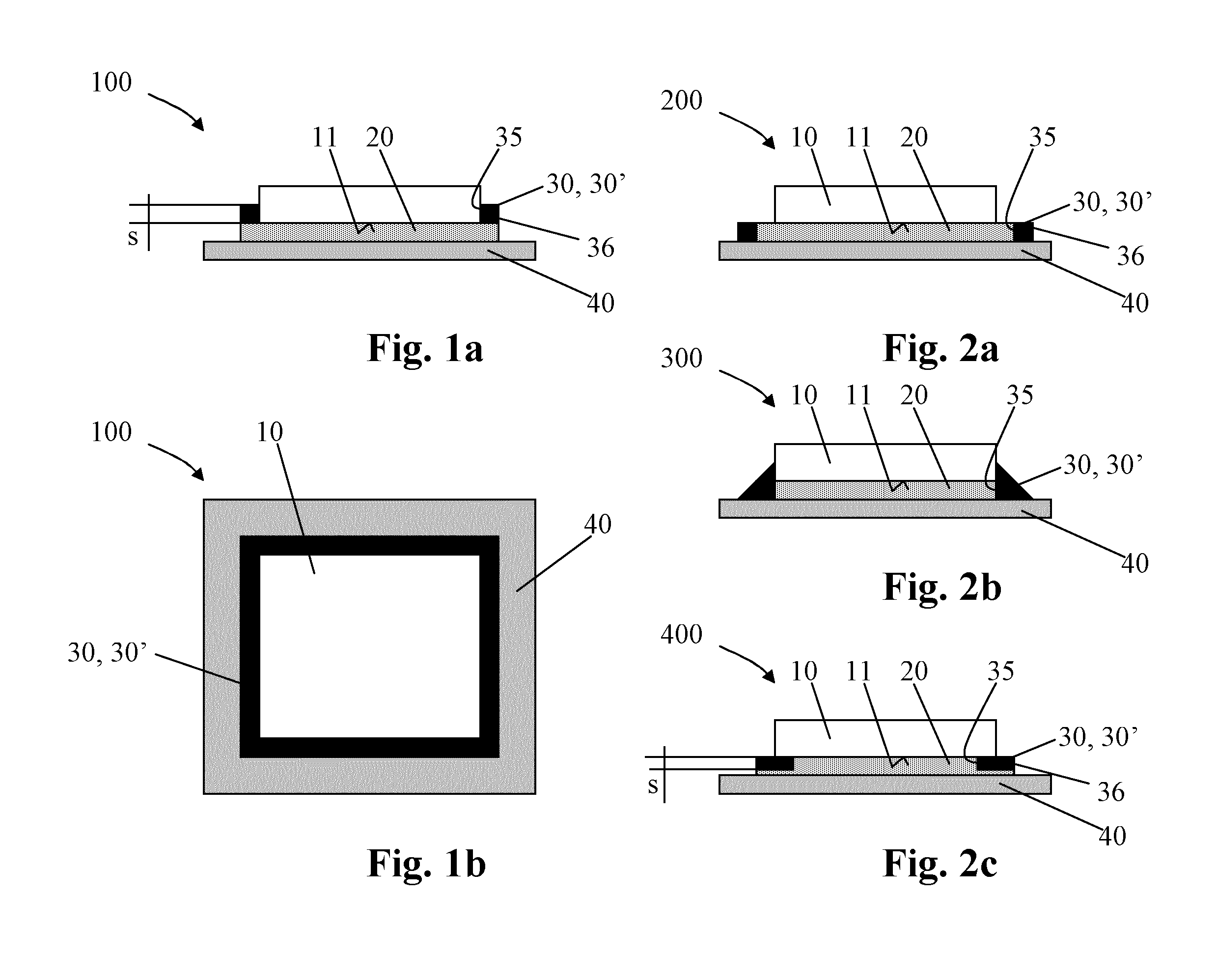
[0031]The FIGS. 1a and 1b show the connection arrangement 100 according to the invention. In order to form the connection arrangement 100, a circuit substrate, for example a DBC substrate, is provided. A semiconductor chip 10 is connected in a bonded manner to the DBC substrate. To this end, the semiconductor chip 10 has a connection face 11 on the side facing the DBC substrate 40. The connection face 11 serves, for example, to electrically contact the semiconductor chip 10 and / or to cool the same. In order to form the bonded connection, a sintered layer 20 consisting of silver is disposed between the connection face 11 and the DBC substrate. For this purpose, the sintered layer 20 can, for example, be present in paste form and be applied to the DBC substrate 40 by means of know paste printing methods. The sintered layer 20 can likewise be formed as a sintered molded part and be applied to the DBC substrate 40 in a form that is then solid and fitted to the connection face 11. In the...
second embodiment
[0035]In the inventive connection arrangement pursuant to FIG. 2a, the solder layer 30 is applied laterally adjacent to the sintered layer 20 on the DBC substrate. As a result, the reinforcement layer 30′ formed after the thermal treatment joins in a bonded manner with the sintered layer 20 as well as with the DBC substrate. In addition, the inner boundary 35 delimits the lateral surface expansion of the sintered layer 20.
[0036]The third exemplary embodiment of the inventive connection arrangement 300 corresponding to FIG. 2b resembles the second embodiment. In contrast thereto, the sintered layer 20 in the third embodiment is substantially flush with the connection face 11 or with the housing of the semiconductor chip 10. In addition, the solder layer 30 is formed in the layer thickness thereof at least in the region of the housing of the semiconductor chip 10 in such a way that at least a minimum height of the housing is surrounded on all sides by a portion of the solder layer 30 ...
PUM
| Property | Measurement | Unit |
|---|---|---|
| thickness | aaaaa | aaaaa |
| thickness | aaaaa | aaaaa |
| thickness | aaaaa | aaaaa |
Abstract
Description
Claims
Application Information
 - R&D
- Intellectual Property
- Life Sciences
- Materials
- Tech Scout
- Unparalleled Data Quality
- Higher Quality Content
- 60% Fewer Hallucinations
Browse by: Latest US Patents, China's latest patents, Technical Efficacy Thesaurus, Application Domain, Technology Topic, Popular Technical Reports.
© 2025 PatSnap. All rights reserved.Legal|Privacy policy|Modern Slavery Act Transparency Statement|Sitemap|About US| Contact US: help@patsnap.com

