
Semiconductor device

Active Publication Date: 2014-08-21
X FAB SEMICON FOUNDRIES
View PDF14 Cites 2 Cited by
  • Summary
  • Abstract
  • Description
  • Claims
  • Application Information

AI Technical Summary

Benefits of technology

The present invention aims to provide a MOSFET structure that has lower switching power loss, improved uniformity and reproducibility, lower specific on-resistance, and the advantage of self-aligning with a substantially constant gate to drain capacitance. These technical effects can be achieved by increasing the thickness of the gate to drain dielectric, adding a second dielectric layer, and reducing the bottom oxide thickness. Additionally, the invention allows for the use of shorter channel lengths, which can result in a lower specific on-resistance, reduced minority carrier diffusion current, and reverse recovery charge Qrr.

Problems solved by technology

However, it is to be understood that not all embodiments necessarily satisfy all (or any) of the above needs.
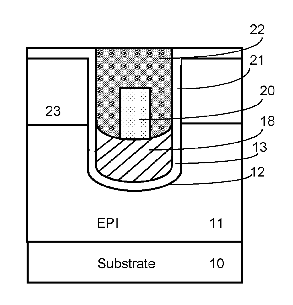
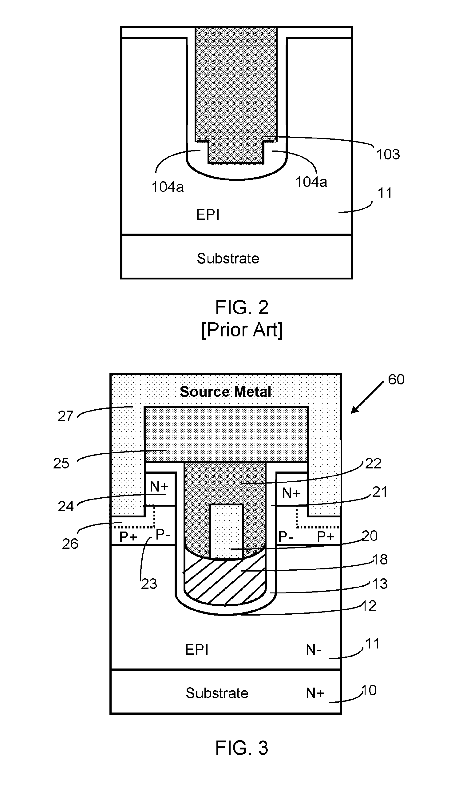
In trench MOSFETs, a relatively large portion of the switching power loss may be due to Miller capacitance, which is a parasitic capacitance effect due to a rising drain current in the MOSFET active state.
In the prior art case of FIG. 1A-1B it is difficult to control the bottom oxide thickness.

Method used


Image

  • Semiconductor device
  • Semiconductor device
  • Semiconductor device

Examples


Embodiment Construction

[0014]One issue is uniformity of the thickness of the TBO. If the TBO thickness is not uniform, the threshold voltage Vth and the on-resistance value may be (very) unstable. In prior art devices such as shown in FIGS. 1A and 1B, the bottom oxide thickness T2 (FIG. 1B) corresponds to the deposited silicon oxide thickness T1 (FIG. 1A) so it is difficult to achieve uniformity of the thick bottom oxide thickness.

[0015]Certain embodiments of the present invention aim to optimize the relative position of what we will refer to as the “gate electrode bottom line” and the “BODY bottom line” in a trench gate Power MOSFET with thick bottom oxide (TBO). Depending on the configuration of the device, there may be a very small overlap between the silicon oxide deposited in the trench and a BODY region of the device. This small overlap may be defined as the height of the top of the silicon oxide deposited in the trench (the TBO)—the “gate electrode bottom line”—minus the height of the top of an epi...


PUM


Abstract

A trench MOSFET including: an epitaxial layer; a body region on the epitaxial layer, the body region and the epitaxial layer forming a first interface; a trench; a trench bottom oxide in the trench; and polysilicon in the trench, the trench bottom oxide and the polysilicon forming a second interface; where the first and second interfaces are substantially aligned or are at substantially the same level.

Description

TECHNICAL FIELD[0001]The present invention relates to semiconductor devices such as high-frequency, high speed switching or power devices and a method of manufacturing the semiconductor devices. The invention particularly relates to trench MOSFETs, in particular to trench Power MOSFETs.BACKGROUND[0002]Power trench MOSFETs are widely used as switching devices in many electronic applications. A parameter in trench power MOSFETs is the total gate charge. In some applications of conventional trench power MOSFETs, such as DC-DC converters, the lower the gate charge the better the efficiency of the overall design. In switching applications a relatively high proportion of power loss is due to gate to drain capacitance (Miller capacitance). Thus an effective way to lower the Miller capacitance is to increase the thickness of the gate to drain dielectric.[0003]FIG. 1A-1B and FIG. 2 are cross-sectional views illustrating prior art trench MOSFETs. As is known in the prior art, a trench 112 is ...

Claims


Application Information

Patent Timeline
IPC IPC(8): H01L29/423H01L29/78
CPCH01L29/7827H01L29/4236H01L29/42368H01L29/66734H01L29/7813
Inventor JEONG, YONG HUNBONG, BUI NGOTAY, YEN THINGMANSO, ILIYANA
Owner X FAB SEMICON FOUNDRIES
Learn More